1. CdTe Photovoltaics
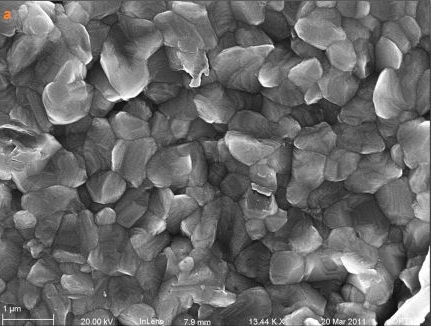
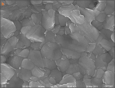
The goal of the continued research in this field is to achieve low cost mass production while retaining and improving the efficiency of the solar cells. The key parameters which affect the efficiency of a solar cell include the optical and electrical properties of the various layers. The interface between CdTe- CdS and the roughness of these layers plays an important role in determining the fill factor of the cells. CdTe grown by various techniques like physical vapor deposition and sol gel have shown high surface roughness with pinholes after NP treatment. A turning point for thin-film CdTe performance was the application of a post deposition air-heat treatment of CdTe/CdS structures with cadmium chloride vapors.
2. Effects of Cadmium Chloride Heat Treatment
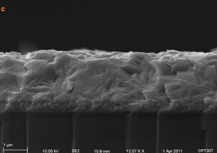
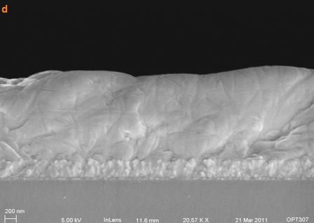
In a typical heat treatment, the as grown CdTe films on glass/ITO/CdS substrate is exposed to Cadmium chloride/oxygen vapor mixture by maintaining a constant vapor pressure of Cadmium chloride over the surface of the film.The treatment improves the overall performance of the solar cells and appears to improve the yield and uniformity of devices[2]. It also enables fabrication of pinhole free ultrathin CdTe/CdS structures resulting in lower fabrication costs.[3]
Characterization Techniques
1. Sample Preparation
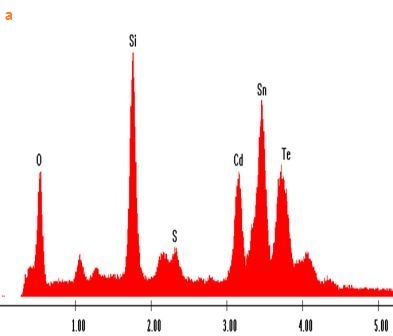
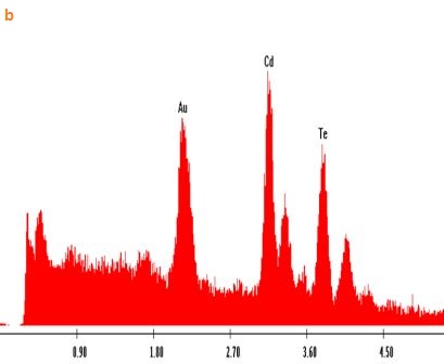
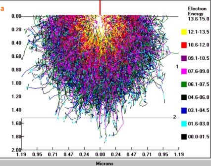
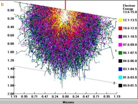
The as prepared samples were sputter coated with gold in order to make them sufficiently conducting for electron microscopy. Typically a deposition time of 60 seconds and a current of 15 amperes was used for depositing gold.Atomic force microscopy was performed on the samples without any sample preparation. Necessary precautions were taken during sizing of the samples for both AFM and electron microscopy.
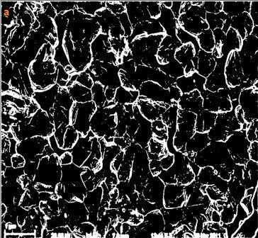
2.Atomic Force Microscopy
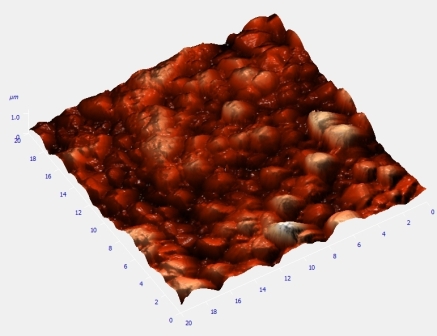
Figure 1:Atomic force micrograph of CdTe showing the rough surface of the as prepared sample.
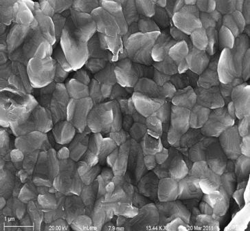
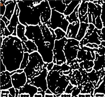
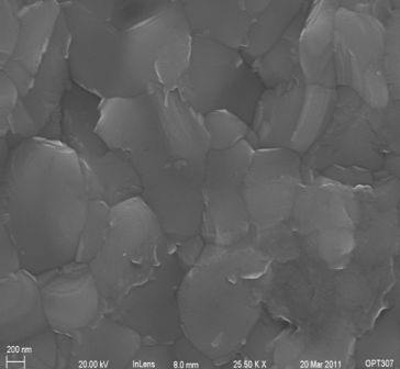
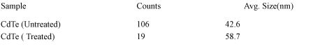
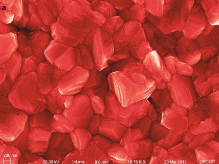
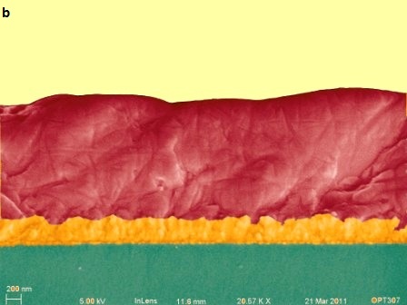
3. Secondary Electron Microscopy
|