The uniformity of a coating over a micro-structured surface such as a diffraction grating will vary depending on the deposition method used. Three different deposition methods were used to coat an optical grating with metal films and each method was subjectively analyzed. Six microscopic techniques were employed to analyze the deposition methods.
Grating samples provided by Brittany Taylor2, Heather Howard2 of the Laboratory for Laser Energetics, were coated using the deposition methods detailed below. Each respective sample was then broken to expose the cross-section and then over coated with a 1-2nm layer of platinum to prevent charging during Scanning Electron Microscope (SEM) imaging.
Sputtering:
- Five 100nm alternating layers of indium-tin-oxide (ITO) and Silicon (Si) applied.
Evaporation:
- Five 100nm alternating layers of silver (Ag) and aluminum (Al) applied.
Atomic Layer Deposition (ALD):
- One 100nm layer of platinum (Pt) applied.
-Secondary Electron (SE) Imaging: Imaging technique which provides information about morphology and surface topography information. Provides the highest resolution images.
-Backscatter Electron (BSE) Imaging: Useful for determining differences in atomic weight (Z-value) within a sample as high Z materials will produce more backscattered electrons. Lower resolution than secondary electron imaging.
-Sputtering Sample Prep: Non-conductive samples must be made conductive by sputtering a thin metal film over the substrate to avoid charging. Charging of the sample will lead to imaging artifacts and degradation.
-Colorization: Color is added after the micrograph is taken to identify areas of interest and increase visual appeal.
-Stereo Pair: Two images are taken at different angles, colored and combined into one image. While wearing red/blue filtered glasses a 3D effect is created for the viewer.
-Focused Ion Beam (FIB): The focused ion beam can be used to cut away material and expose inner features of a sample.
The grating provided was 500nm tall pillars at 1750 lp/mm etched from a SiO2 layer.
 |
 |
|
Figure 1: A secondary electron image of the substrate. The pillars were composed of SiO2. It was over-coated with 1-2nm of Pt to prevent charging. |
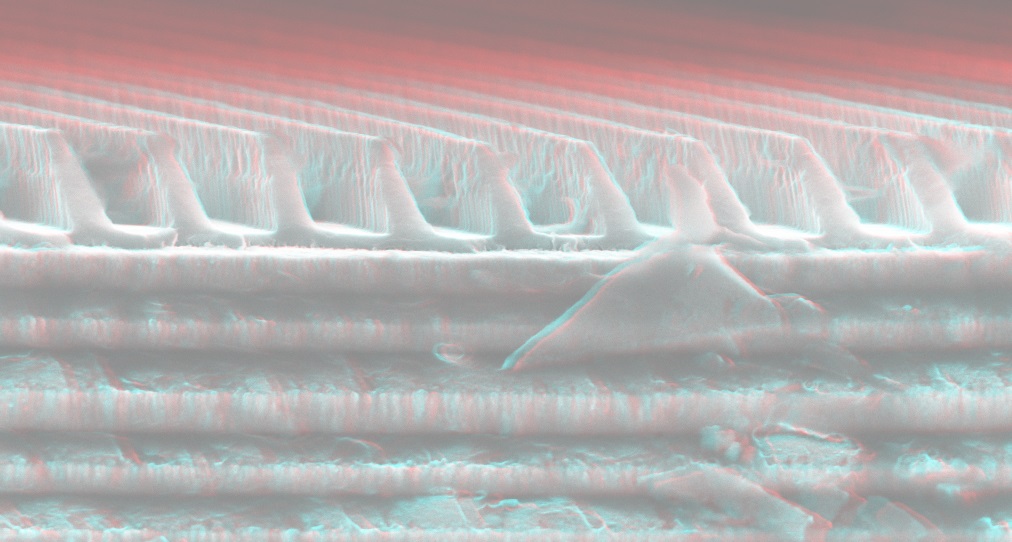
Figure 2: Stereo pair of the substrate to show depth. |
 |
|
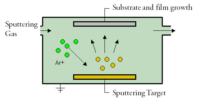
Figure 3: Argon gas is ionized and accelerated to a target. The argon ions impact the target causing ejection of the target material, which will coat the substrate. The sputtered material is also likely to scatter off of other argon atoms allowing it to more uniformly coat surface features. http://en.wikipedia.org/wiki/File:Sputtering.gif |
 |
 |
|
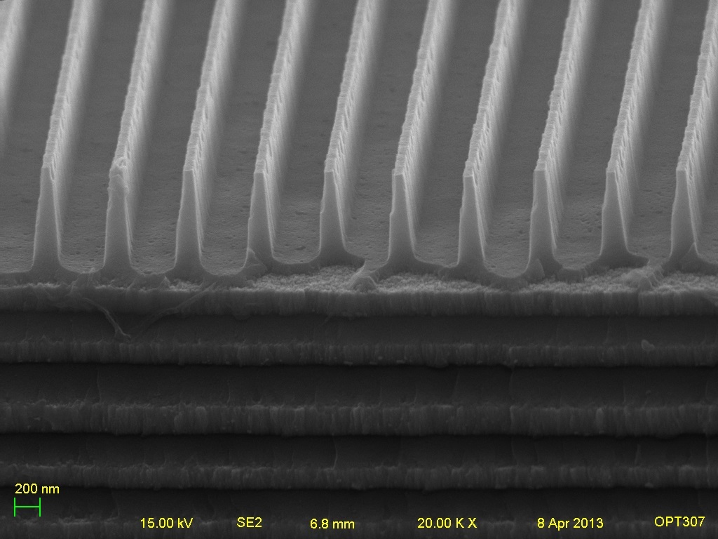
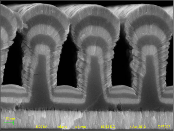
Figure 4: A secondary electron image
of a cross-section of the ITO and Si sputter coated
grating.
|
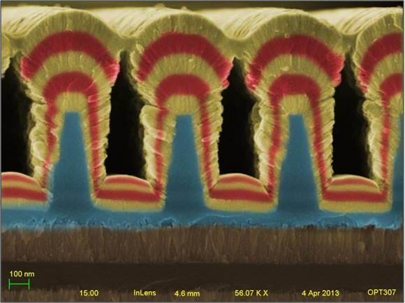
Figure 5: A colorized secondary electron image highlighting the different materials. red-Si, yellow-ITO, blue-SiO2. |
 |
|
|
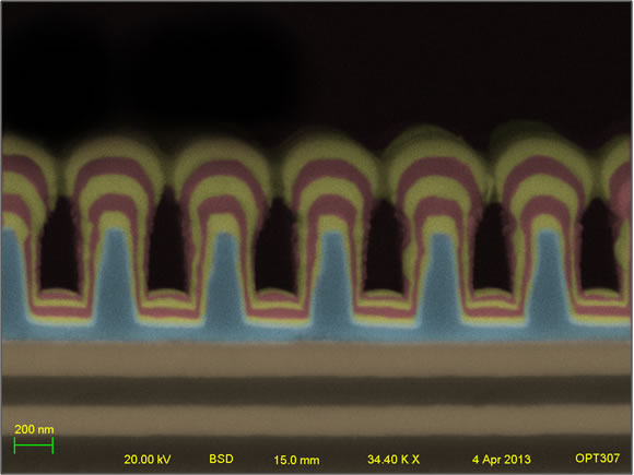
Figure 6: A colorized backscatter image showing differences in the materials based upon atomic weight. Figure 8: Note the decreased resolution compared to the secondary electron image due to the larger interaction volume. |
Figure 8: Interaction volume. |
|
Figure 7: EDAX results of the sample identifying each of the atomic components of Si, In, Sn and O. |
|
Figure 9: A simple diagram of electron beam evaporation. The target material is heated by an electron beam causing a vapor cloud which coats itself onto the substrate above. Evaporation coats by line of sight, where only portions of the substrate normal to the vapor cloud will be coated. http://wwwold.ece.utep.edu/research/webedl/cdte/Fabrication/ |
| Figure 10: A colorized secondary electron image highlighting the different materials (blue-SiO2, green-Ag and purple-Al. Notice how the sides of the pillars were not coated as much when compared to sputtering and ALD. |
Figure 11: A colorized secondary electron image, where the coating has peeled off of the substrate. |
|
Figure 12: A combined secondary and backscatter electron image. Both detectors can be used at the same time to highlight material differences (BSE) while retaining detail (SE). |
|
Figure 13: EDAX result of the sample; material components identified are Ag, Si, O and Al. This EDAX result was also able to identify traces of the Pt used to coat the sample. The small amounts of Cu detected could be due to the electron beam hitting the copper surrounding the crucible. |
|
Figure 14: A diagram of ALD. Precursor gas is introduced into the coating chamber and attaches to the substrate in a single molecular layer . The remainder of the gas is swept away and a second precursor gas is introduced. The second gas reacts with the deposited monolayer leaving behind an atomic layer of the desired material. ALD coatings are very uniform over the entire surface and features. |
|
Figure 16: A secondary electron image of the ALD coated grating. Note the uniformity of the coating over the pillars. |
Figure 17: A secondary electron image of the ALD coated grating. The coating has separated from the substrate. |
|
Figure 18: The grating was cut with a FIB to create a smoother face to observe the coating: (a) shows the FIB etched face, (b) shows the hole that was dug into the substrate, (c) shows the substrate cut with a thicker platinum overcoat to help smooth the cutting process and thus the exposed face. |
||