Temperature measurement at tiny hotspots formed in a biological cell or nanoelectronics is a huge challenge.
For such purposes, the sensing technology must be completely a non-contact one or should involve nanoscale probe to minimize thermal transportation from the object-of-interest to the probe.
Non-contact thermal imaging involves detection of blackbody or thermal radiation emitting from the hot surface.
However, its sensitivity and spatial resolution would be fundamentally limited by high temperatures and diffraction limit of the imaging system (Wavelength/2*Numerical Aperture) respectively.
[1]
2. Luminescent Thermometers
Nanodiamonds (NDs) with nitrogen-vacancy (NV) centers whose overall size is less than 100 nm are potential candidates for temperature nano-sensing.
When a green laser beam is shone on these NV-NDs, they emit red light whose luminescence intensity and lifetime are highly affected by the temperature of surroundings.
Hence, they can be used to analyze the temperature dynamics with nanosecond range temporal and excellent spatial resolution.
[2]
3. Challenge
NV-NDs are more likely to agglomerate and form clusters when dropcasted or spincoated on the sample surface.
Separating individual NV-NDs from those clusters and placing them at a particular location-of-interest is very important to get accurate results.
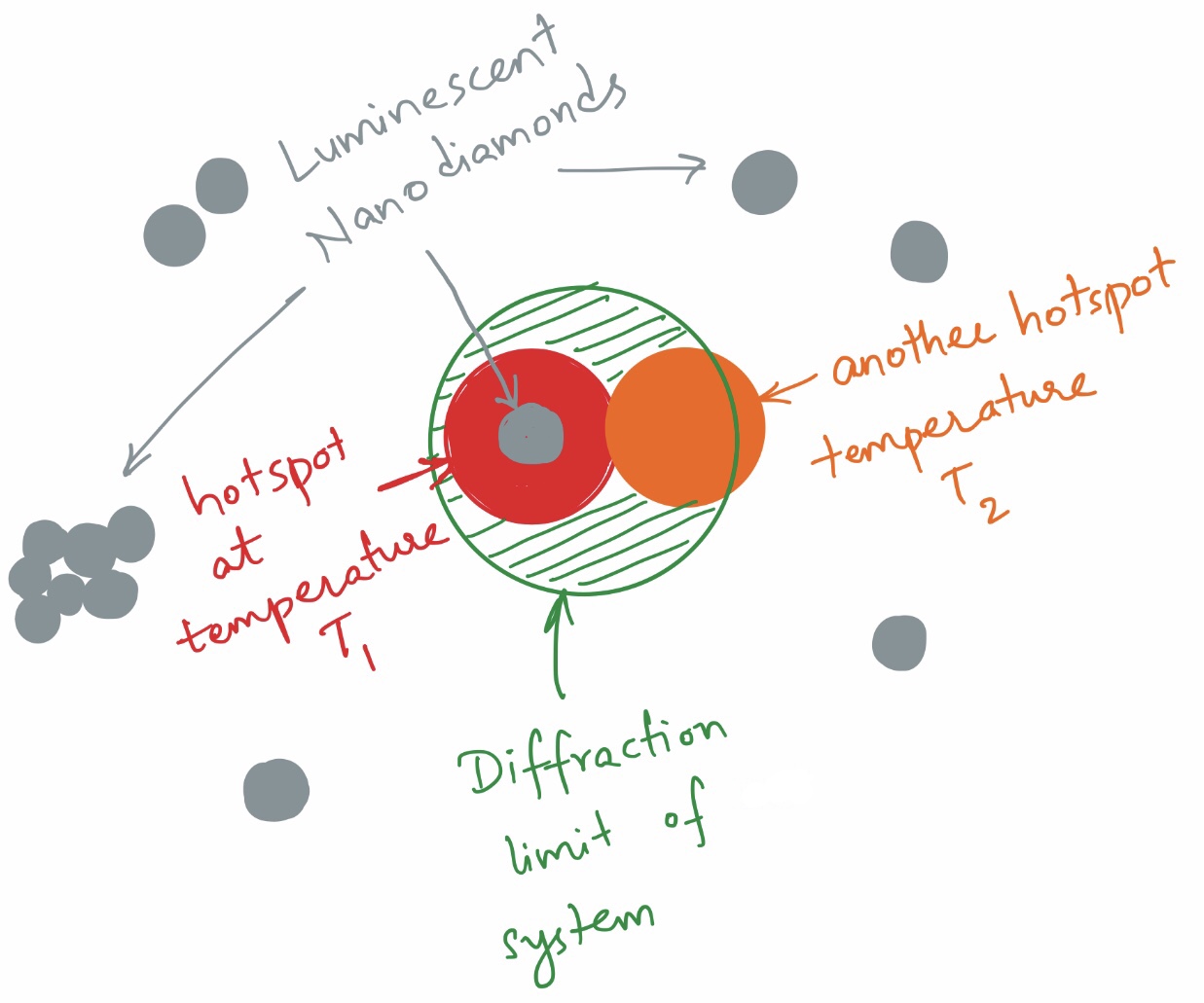
Figure 1:
Schematic to illustrate two different tiny hotspots inside a diffraction limited spot
and the importance of placing a NV-ND at the location-of-interest.
Another concern is that no two NV-NDs are alike though synthesized in similar conditions. Hence, commercially available NV-NDs pre-coated with a thin SiO2 shell were chosen for smooth maneuvering on the flat surface of the substrate. The main goal of this project is--
(a) to characterize the purchased NV-NDs and
(b) demonstrate a successful nanomanipulation using an Atomic Force Microscope (AFM).
Methods and Results
1. Transmission Electron Microscopy (TEM)
Dispersion of NV-NDs in ethanol as received from the vendor was further diluted to achieve
1/25 ppm concentration. Then a tiny drop of that diluted NV-NDs dispersion was dropcasted
onto a TEM grid.
The Bright-field images taken at various magnifications
illustrate the overall average size of NDs with silica shell is well within the 100 nm range
with thickness of Silica shell ranging from 10-20 nm. Differently diffracted electron beam
through the amorphous silica coating caused a good contrast between NV-ND at core
and silica around it.
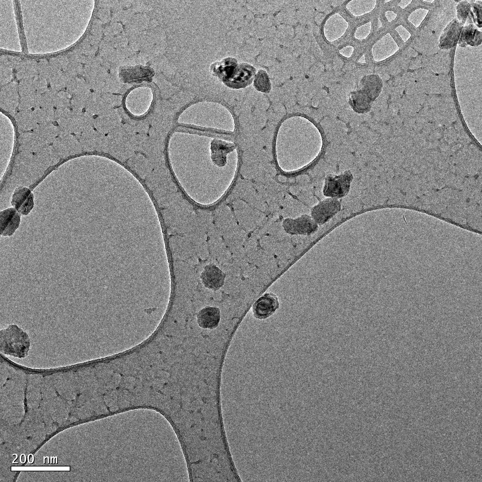
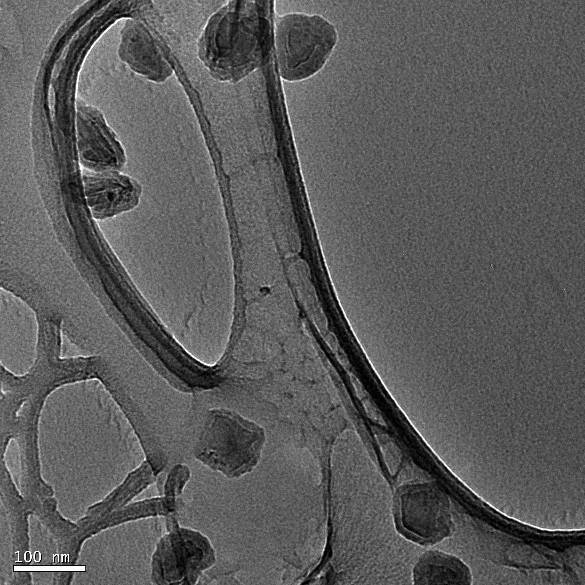
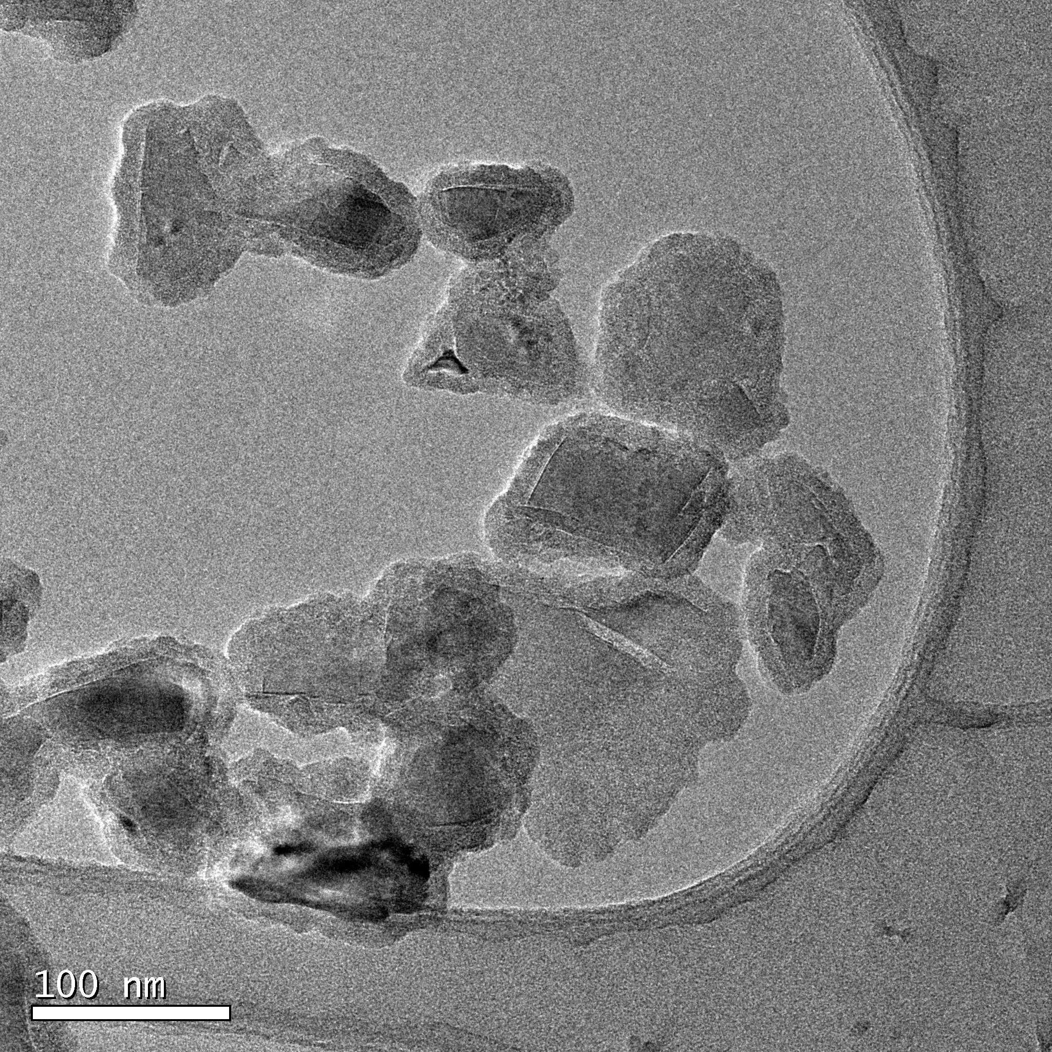
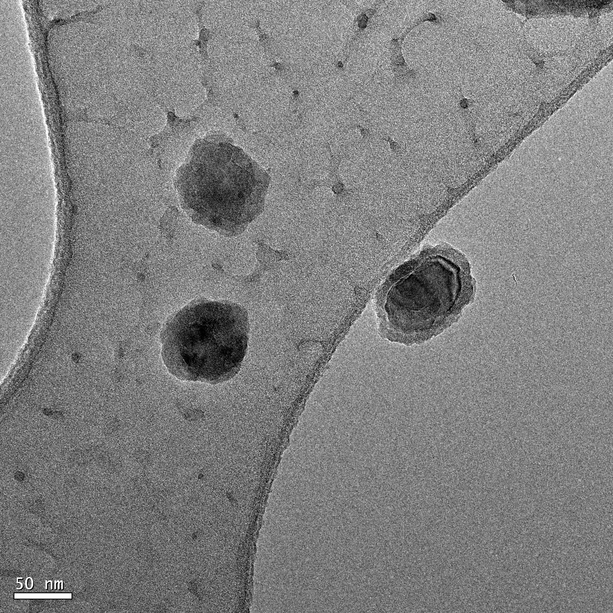
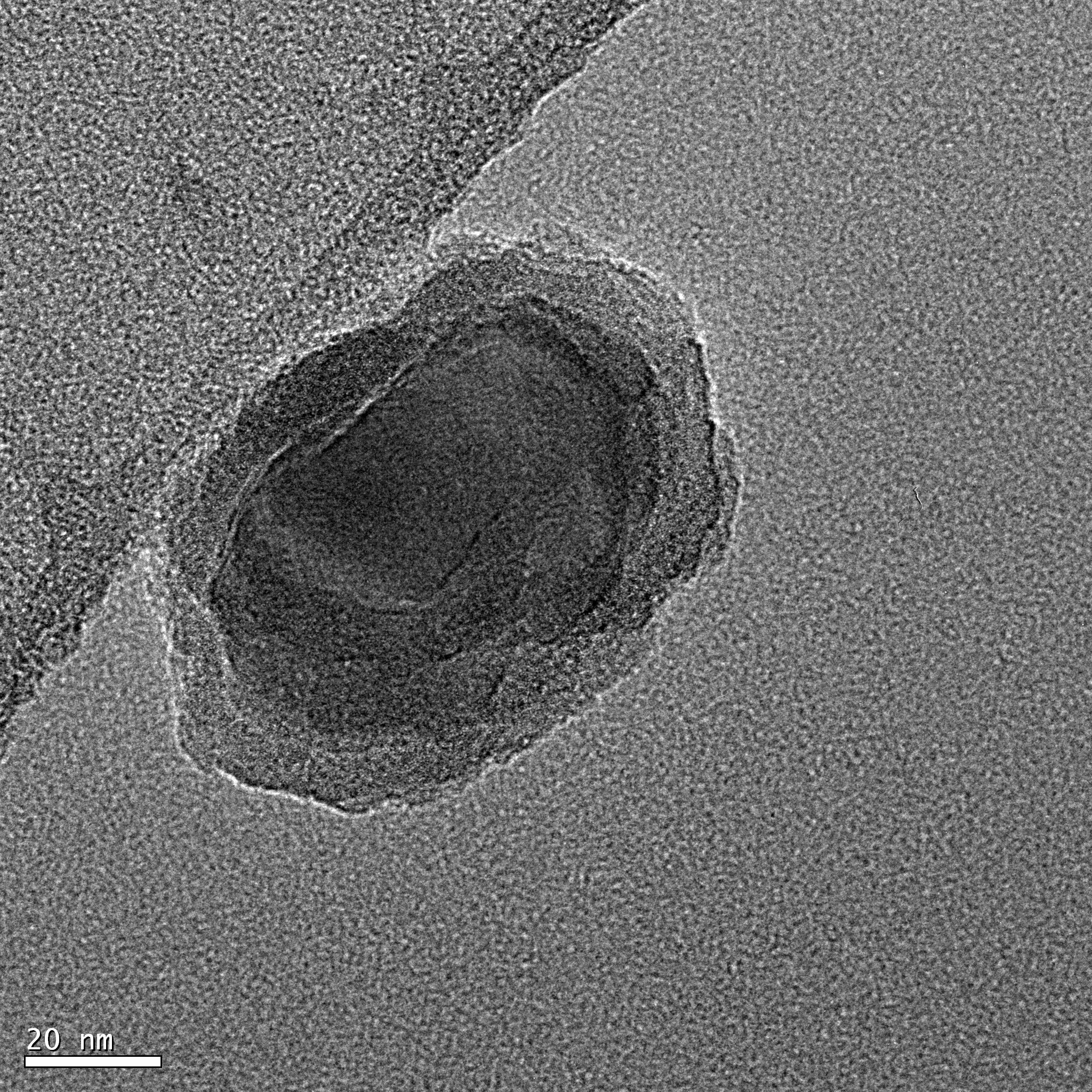
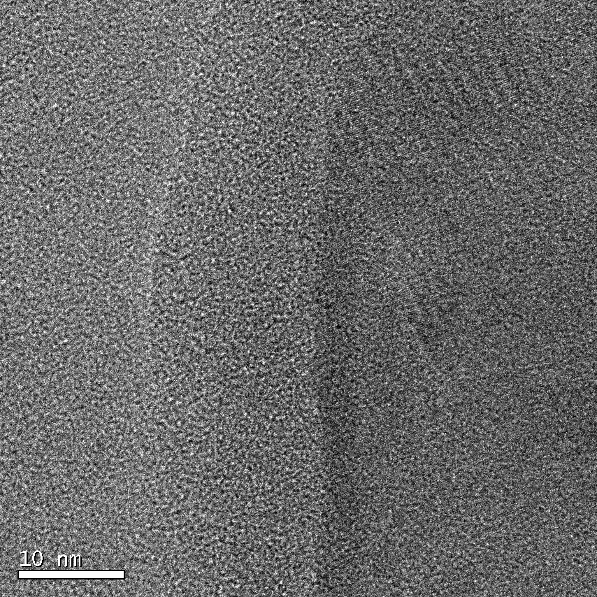
Figure 2:
Bright-field images of some random NV-NDs taken at different magnifications
to establish the size range and coating thickness.
2. X-ray Spectroscopy
Now that the average size of NDs was ensured to be under 100 nm range, a quality analysis
was performed using Energy Dispersive Spectrometry (EDS) in the TEM. Scanning TEM (STEM) was
invoked to obtain a dark-field image after which drift corrected spectral maps were taken.
Images shown below indicate two sets of analyses where shells clearly consisting of Si, O
elements around a diamond core made of C.
Later those individual maps were overlayed on each other using Photoshop.
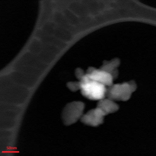
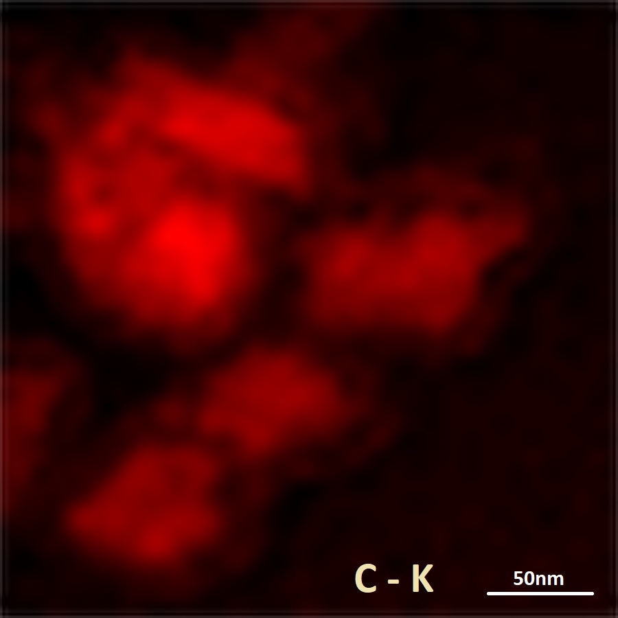
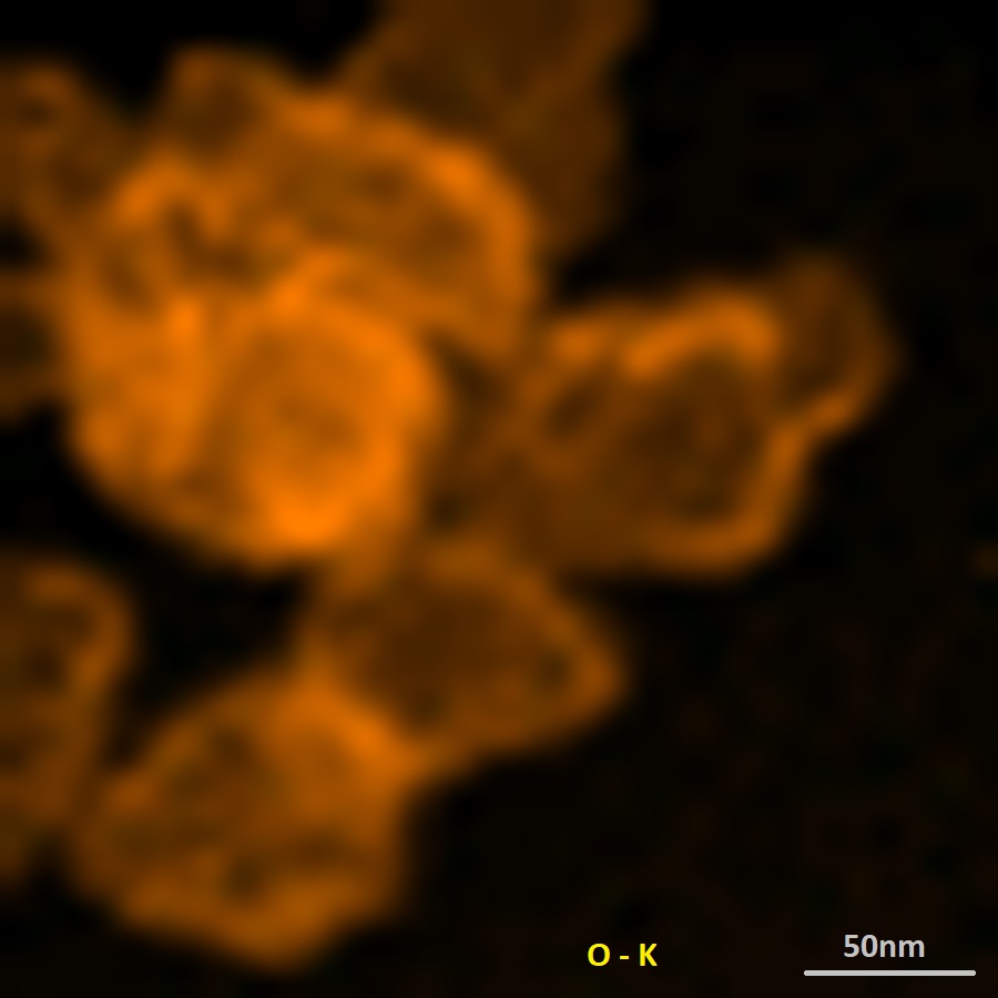
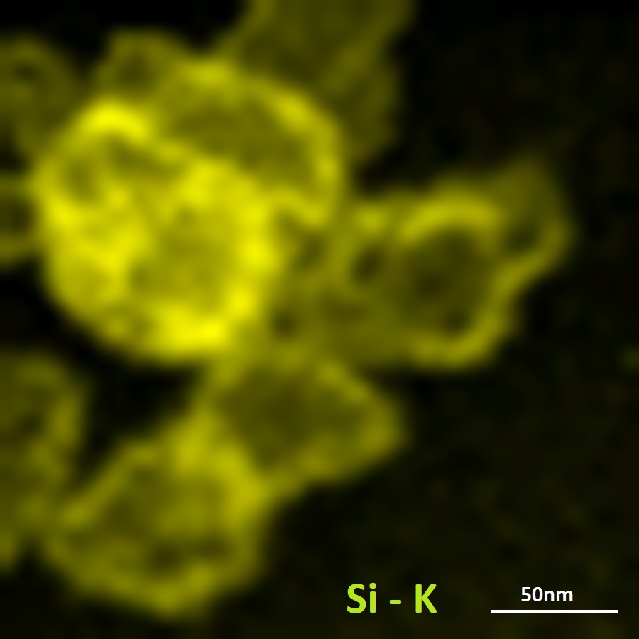
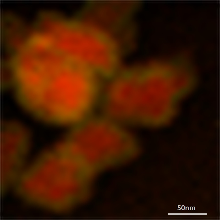
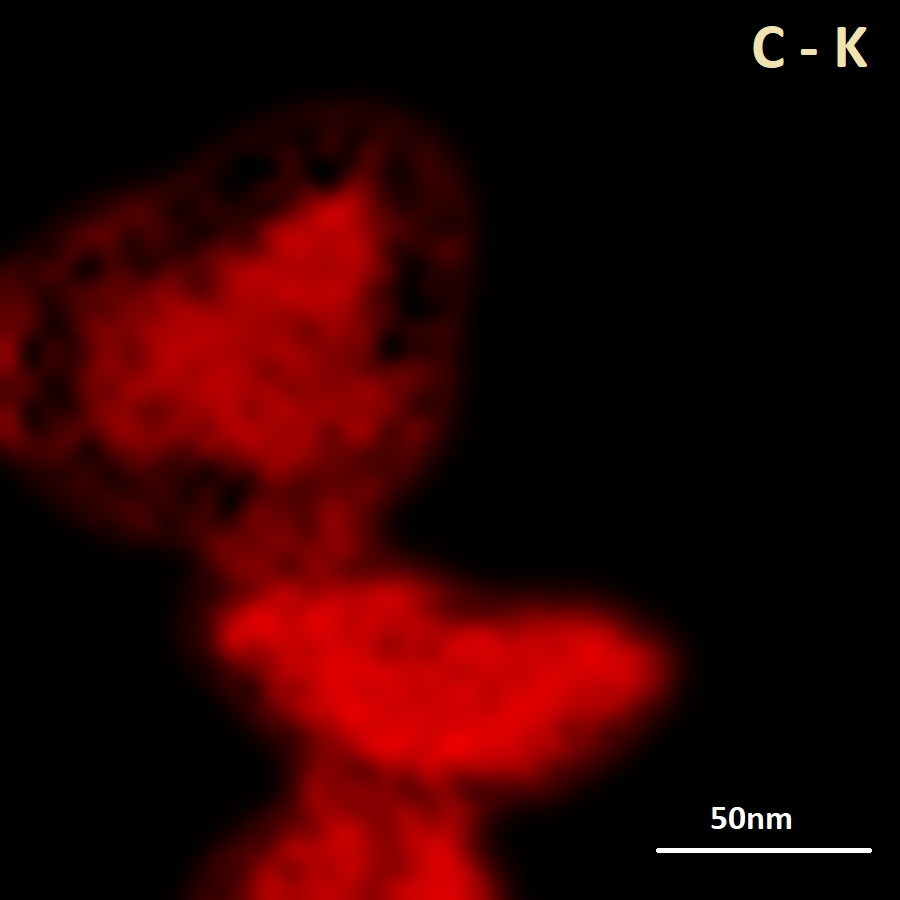
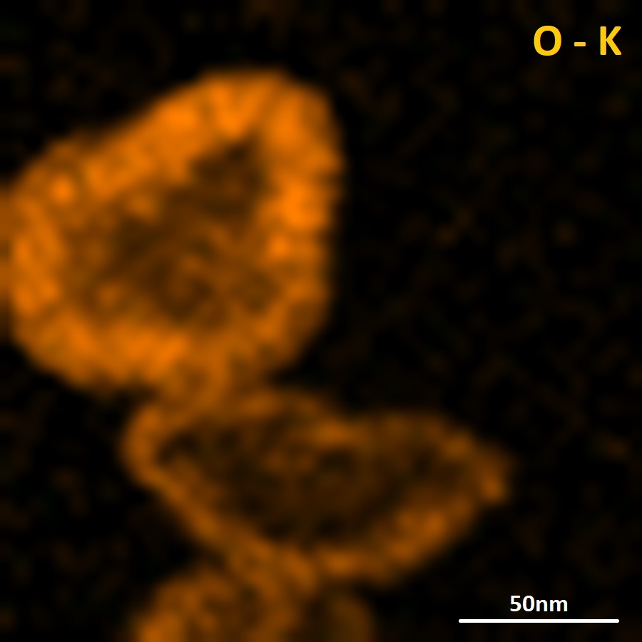
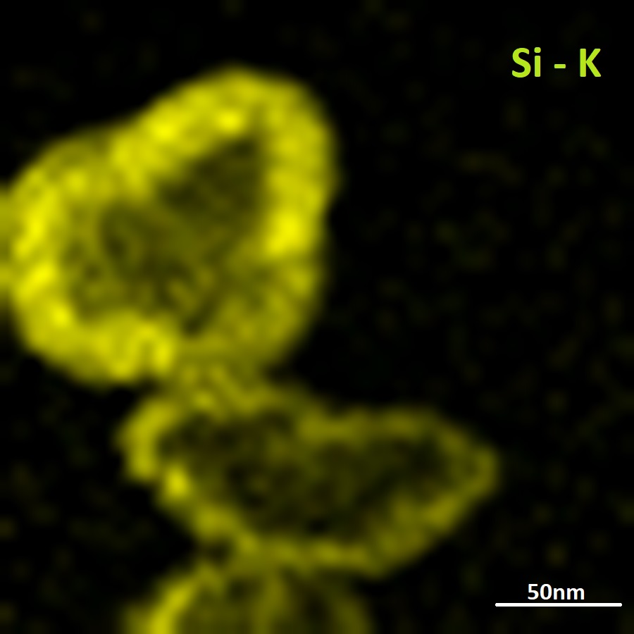
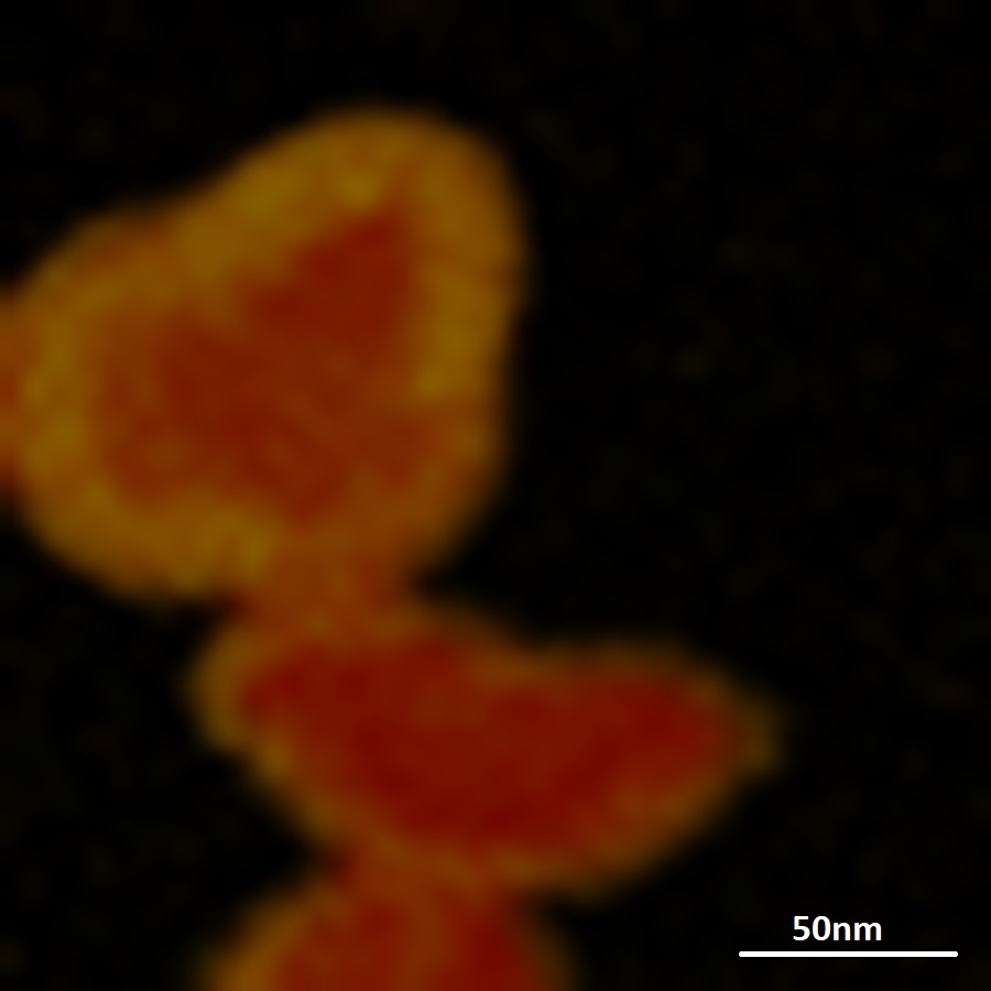
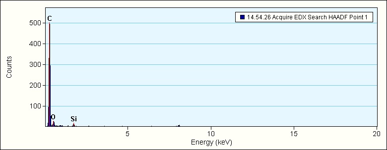
Figure 3:
X-ray microanalyses done for two sets of NDs confirming the presence of silica shell around each ND .
3. Sputter-coating
The substrate chosen for this project was a 22 mm*22 mm clean glass coverslip.
As glass is a non-conducting material and builds static surface charging
when imaged under Scanning Electron Microscope (SEM), it was coated with a ~50 nm thin Platinum (Pt)
film using Denton Sputter coater. Later a spin-coater was used to coat this Pt-coated
glass with the previously prepared 1/25 ppm NV-NDs in ethanol.
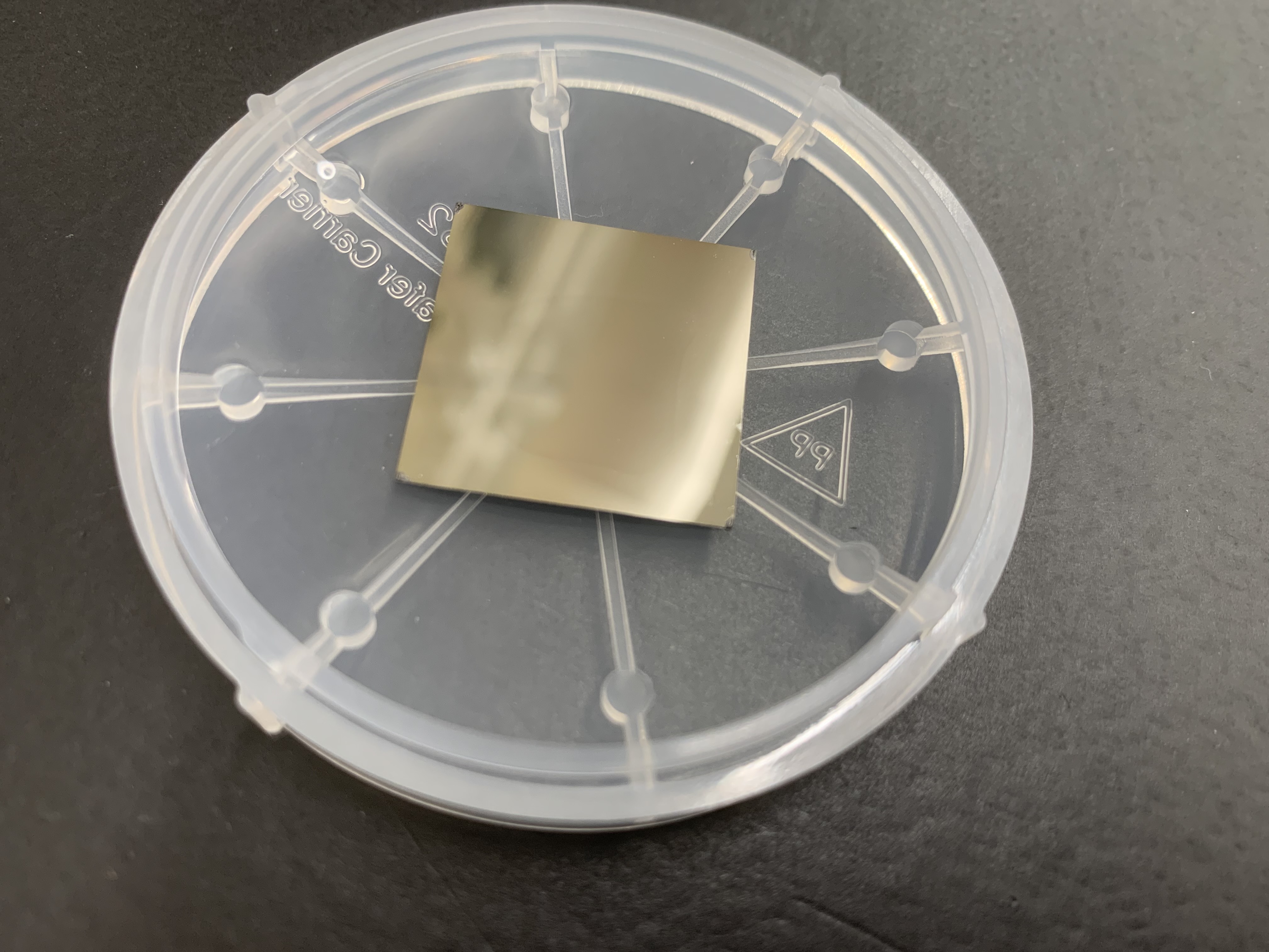
Figure 4:
Pt-coated glass coverslip with NDs spincoated on it.
4. Focused Ion Beam (FIB) Milling
As discussed earlier, each ND is unique in its size, shape and luminescence though they are
all synthesized in the same batch. Additionally, features seen in the scanned images of
Atomic Force Microscope (AFM)
do not always ensure the presence of individual/single NDs.
Sometimes they could also be the dust nanoparticles or two NDs stacked upon one another.
Therefore it is a good practice to double check the NDs under SEM after imaging/manipulating
them under AFM.
The plain featureless surface of Pt-coated glass makes it difficult to locate the same set of
NDs everytime the sample is swtiched between SEM and AFM. Hence fiducial markers were made
using FIB milling to approximately identify and scan the same region when imaged under SEM and AFM.
The images shown below are some of the fiducial markings taken using both SEM and AFM
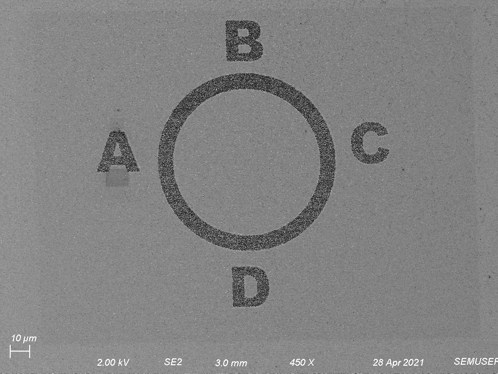
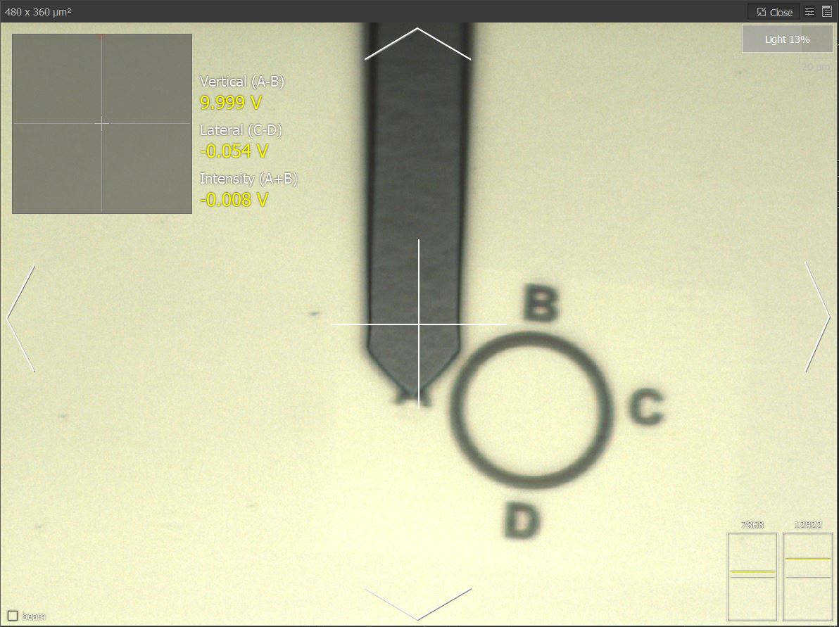
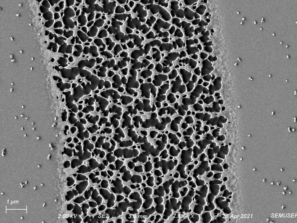
Figure 5:
Comparison between images taken approximately at same location under both SEM and AFM respectively.
The width of each stroke is ~5 microns
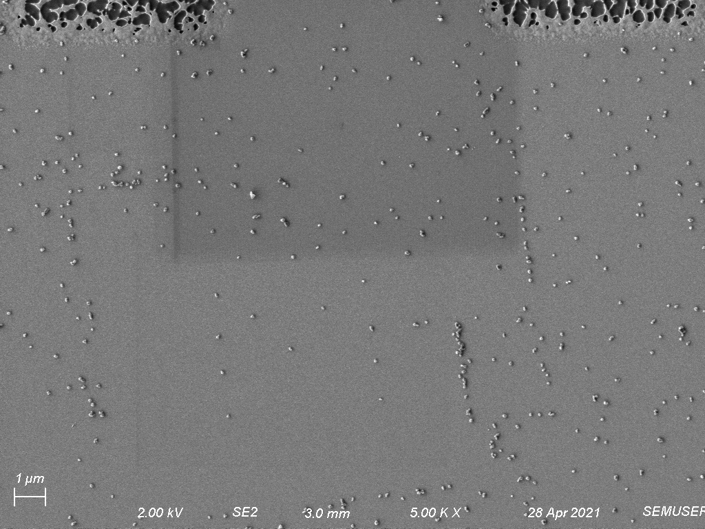
5. Atomic Force Microscope (AFM)
A lot of NDs could be found in any given 10 microns * 10 microns area as shown in Figure 6.
The aim is to separate the closely packed nanodiamonds to a comfortably resolvable distance
i.e., > 1 micron.
(This prevents overlapping of luminescence intensity information coming
from two adjacent single particles during luminescence lifetime measurements.)
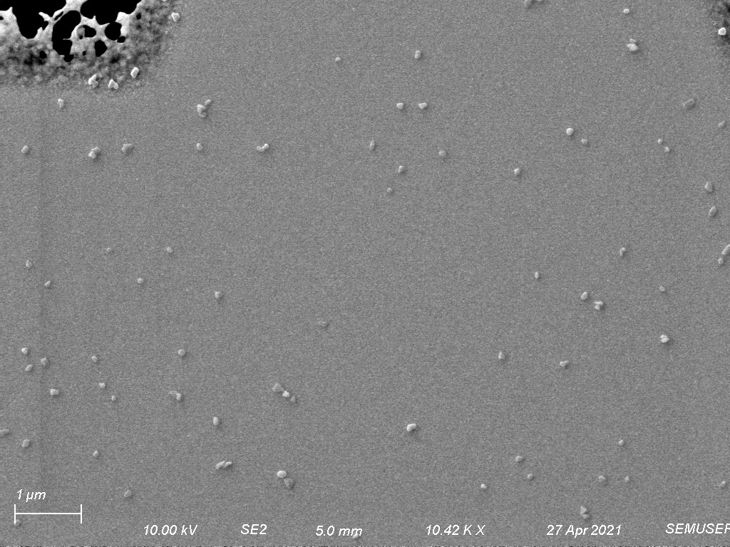
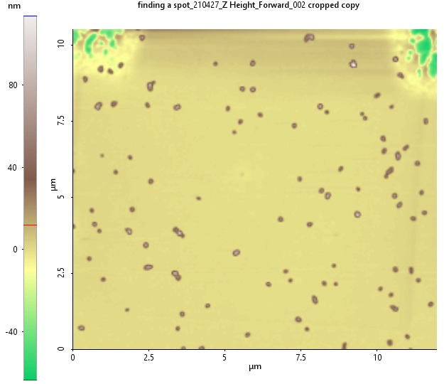
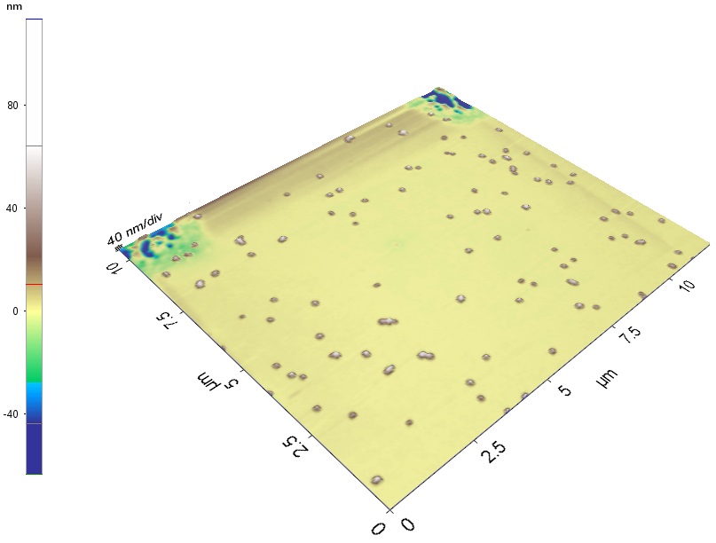
Figure 6:
Comparison between images taken at same location under both SEM and AFM (non-contact mode) respectively.
Scans were made at the bottom of marking 'A'.
Same set of NDs can be found in either cases
Hence, the AFM cantilever tip was engaged in contact mode with a gentle setpoint force of 15 nN.
The NDs that are stuck to the substrate by the weak vander Waal forces can be moved
around by the controlled motion of AFM tip.
This is analogous to pushing a pebble using a vertical stick in real life.
To notice any observable change in the position of NDs, a space 10 * 10 sq.microns was cleared
by pushing all the NDs to the sides as shown in Figure 7.
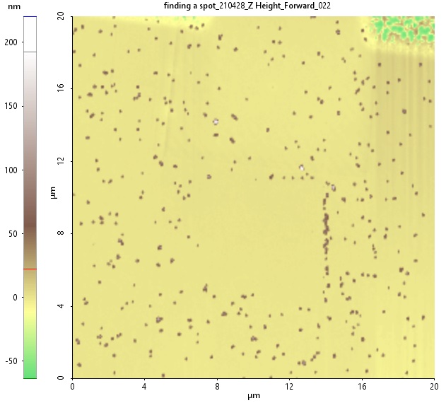
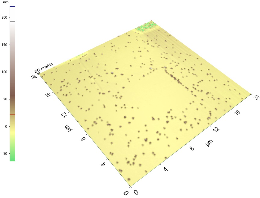
Figure 7:
Made room to observe the changes in positions of NDs
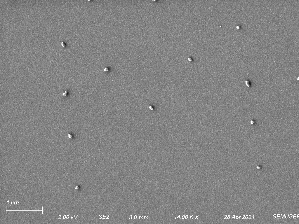
6. Nanomanipulation
Then the NDs at edges were carefully moved as shown in Figure 8. If carefully observed, only
the particle on the bottom right section was moved to a distance of ~2 microns without interrupting the others
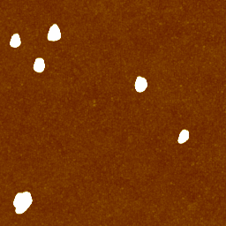
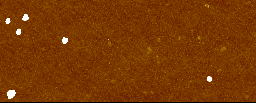
Figure 8:
The AFM scans showing the same set of NDs before and after manipulation
Thus a total of 11 NDs were manipulated into a pattern that looks like 'M' which of course is
highly improbable to form by itself when spin coated.
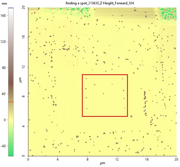
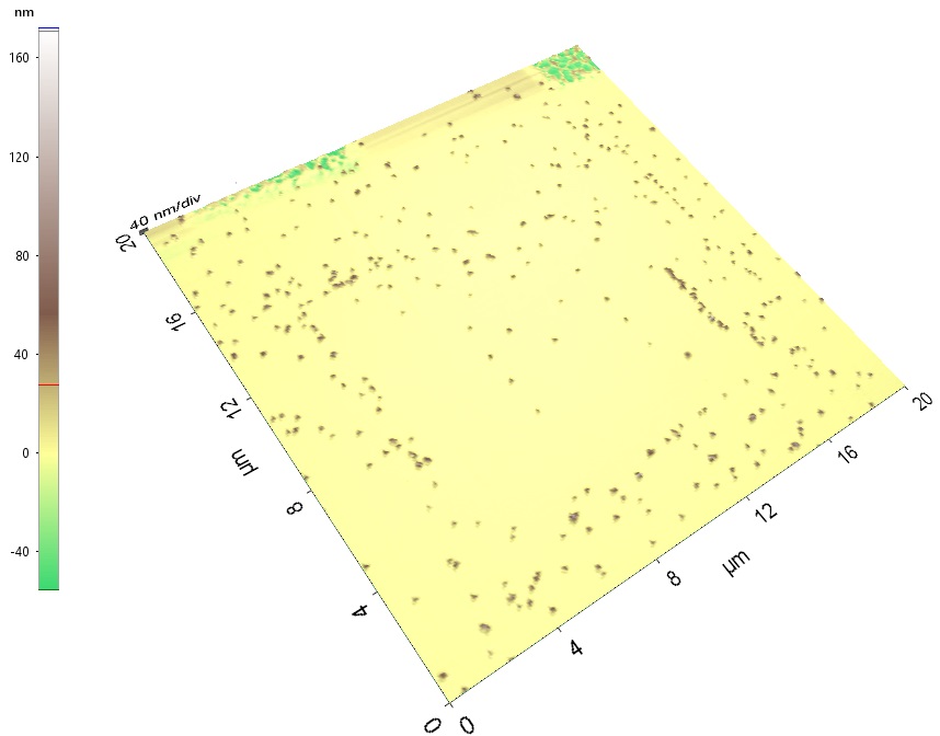
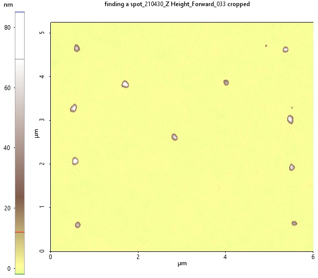
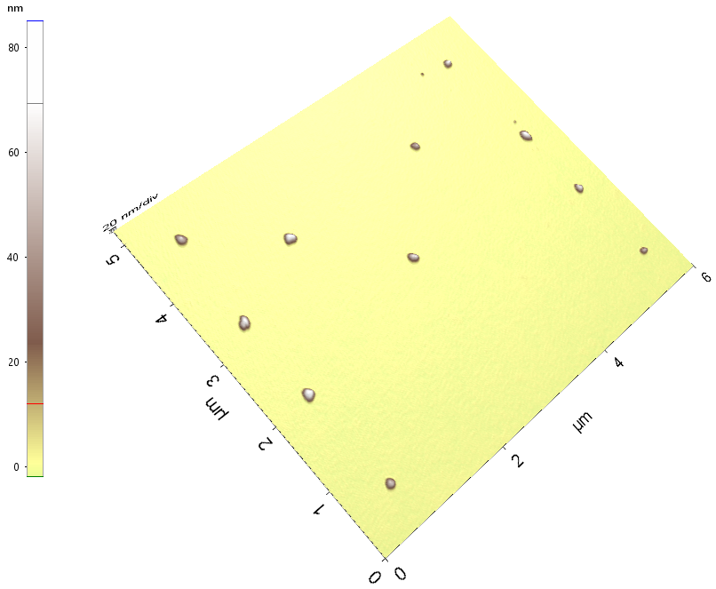
Figure 9:
The AFM scans showing pattern 'M' made using NDs.
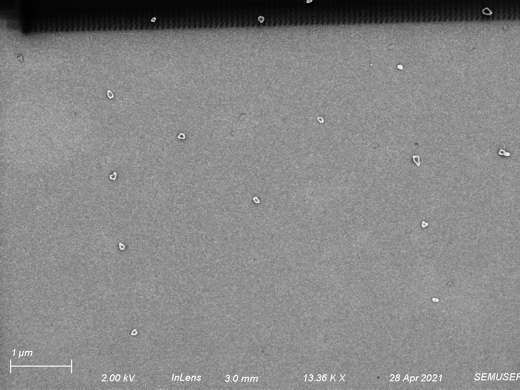
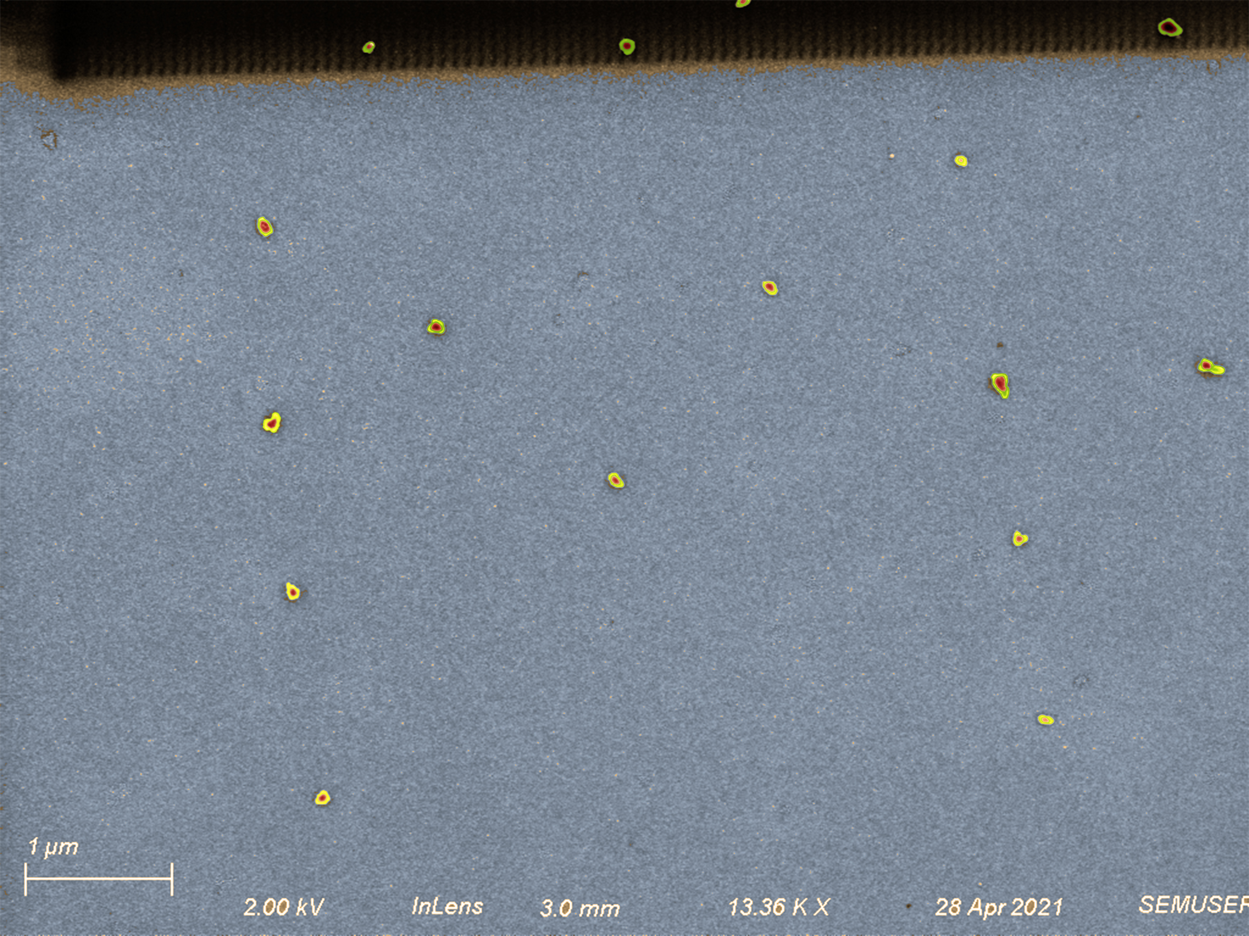
7. Reaffirmation and colorization
After successful manipulation was performed, the pattern was reverified under SEM.
Due to the size scale of NDs and thin Pt-coating,
a short working distance of ~3 mm and low acclerating voltage of 2 kV were used to
obtain micrographs from both SE2 and Inlens detectors.
Due to the close working distance, the Inlens detector produced great contrast
differentiating between what seemed like diamond core and silica shell.
Hence the image taken from Inlens detector was colorized in photoshop to accentuate those
differences bewteen diamond core and silica coating.
| | | | | | | | | |