Imaging with a charged beam in the high vacuum environment within the SEM gives rise to many challenges throughout the process, with one of the most pervasive being the imaging of insulators. When the incident electron beam has no conducting path to flow to ground — typically the metal sample holder — a charge potential builds up on the surface of the sample. This effect, cleverly dubbed "charging," gives rise to many problems in the imaging of samples, from saturating the surface of the sample and obscuring topological information, to causing problems with contrast, blurring, or beam deflection. This is most commonly seen with uncoated insulating samples, however it can occur with any sample that is isolated from ground. Ordinarily, it is an effect that would be avoided as much as possible, and can be mitigated through the use of a lower accelerating voltage beam, closing down the aperture size, or imaging in low vacuum modes. However, here, it is actually a useful effect that will be leveraged for the creation of electron mirrors.
2. The Electron Mirror Effect
The electron mirror effect is an under-explored, curious phenomenon present in electron microscopy that has been observed since the 1970s. Usually, it's an anomalous effect that most microscopists seek to avoid. When the surface of a sufficiently electrically isolated sample is saturated with electrons from a highly energetic beam, and then subsequently driven with a beam at a lower accelerating voltage, the beam will be redirected and imaging of the interior of the SEM chamber will suddenly appear. Instead of interacting with the surface of the sample and generating Secondary Type I electrons, the beam electrons are instead redirected to the interior of the sample chamber and generate Secondary Type III electrons (see Fig. 1). These electrons can then be detected using the Everhardt Thornley (SE2) detector, which will attract the electrons utilizing a reverse-biased Faraday cage.
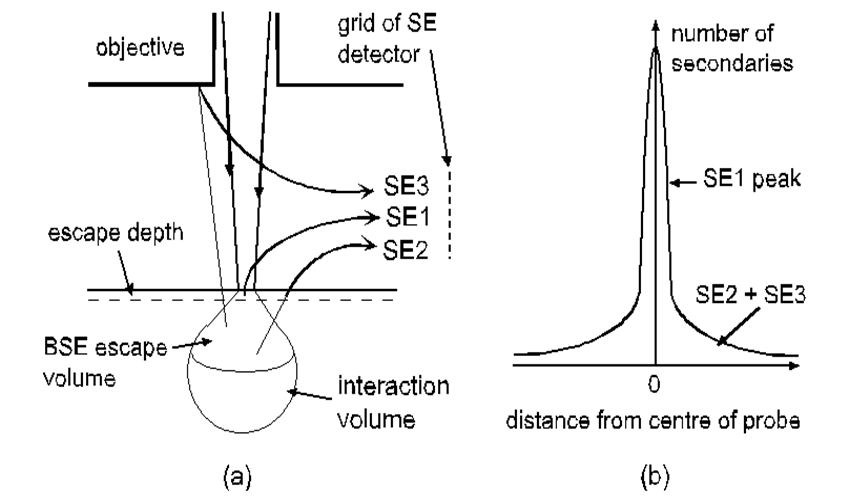
Figure 1: Types of secondary electron signals present in the SEM chamber. Secondary Type I electrons emerge from very close to the surface of samples and are typically the primary signal detected when using the SE2 or InLens detectors. Secondary Type II electrons emerge from deeper in the surface of the sample, and Secondary Type III electrons are generated from the interior components of the chamber. Secondary Type III electrons are what are primarily being detected when electron mirroring occurs. Figure obtained from McIntyre [1].
The mirroring effect can be explained by the difference in the potential charge on the surface of the sample (the "mirror") and the voltage of the beam; as the lower energy electrons become closer to the surface of the mirror, the negative potential on the mirror repels the beam electrons from actually coming into contact with the surface of the mirror. This "reflection" of the beam electrons at a virtual surface away from the surface of the mirror allows the mirroring effect to remain intact. It is because of this that it is crucial to charge the surface of the mirror with a high enough accelerating voltage compared to the voltage of the electron beam used for imaging. Otherwise, for example if the charging voltage for the mirror and the imaging voltage of the electron beam were the same or comparable, then the beam electrons and the mirror electrons would be displaced in their interaction, and the mirror would then be destroyed. A more detailed description of the working principles of the electron mirror effect is described in the literature [2].
Understanding the electron mirror effect and charging, it is then straightforward to develop a method for creating an easily reproducible, analytical tool for use inside the electron microscope. Simply, a sample that is isolated from ground can be charged with a sufficiently high accelerating voltage beam through an aperture which is opened at its largest diameter to allow the surface to be bombarded with electrons. Once the surface is sufficiently charged, the aperture can be closed down to a size typical for imaging and the accelerating voltage is lowered significantly. If successful, the mirroring effect should be immediate, and can then be used.
3. Viewing Samples From Multiple Orientations
Although the SEM is incredibly versatile in its imaging capabilities, the tool does have its limitations. Generally, the SEM is best at producing images of a top-down view of the sample. Without having to vent the chamber, remove, replace, and reinsert the sample, it is difficult to obtain images of a single sample at multiple orientations using the electron beam in its standard configuration and mobility aside from some tilting of the sample stage. This process can become increasingly lengthy (and subsequently costly) and increases the possibility of damaging the sample when remounting it. The addition of mirrors within the sample chamber can vastly enhance the imaging capabilities of the SEM, and greatly reduce the time spent when attempting to obtain information from multiple orientations of samples, which can be especially useful for abnormal samples where particular geometries within the chamber may be an issue.
Previously, within the scope of this course, electron mirrors have been created and demonstrated by Greg Savich in 2008 [3] and Greg Pilgrim in 2011 [4]. However, both of these projects involved the imaging of a sample at a fixed geometry, where both the sample and the electron mirrors were mounted on the sample stage within the SEM. The primary goal of this project was to separate the electron mirror from the sample stage in order to utilize the full mobility of the stage to image regions of samples ordinarily unable to be interrogated by the electron beam. This was achieved by mounting the mirrors on the micromanipulator arm present in the SEM chamber, allowing for the movement of the mirror and the sample stage independenty of each other and therefore creating a more dynamic tool to image with.
Experimental Methods
1. Sample and Mirror Preparation
In order to create an effective mirror, a small selection of different materials were obtained and prepared. Insulating, semi-insulating, and conducting materials were used to compare the mirroring effect among these sample types, since the electron mirror effect does not require that the mirror be an insulator, but merely isolated from ground.
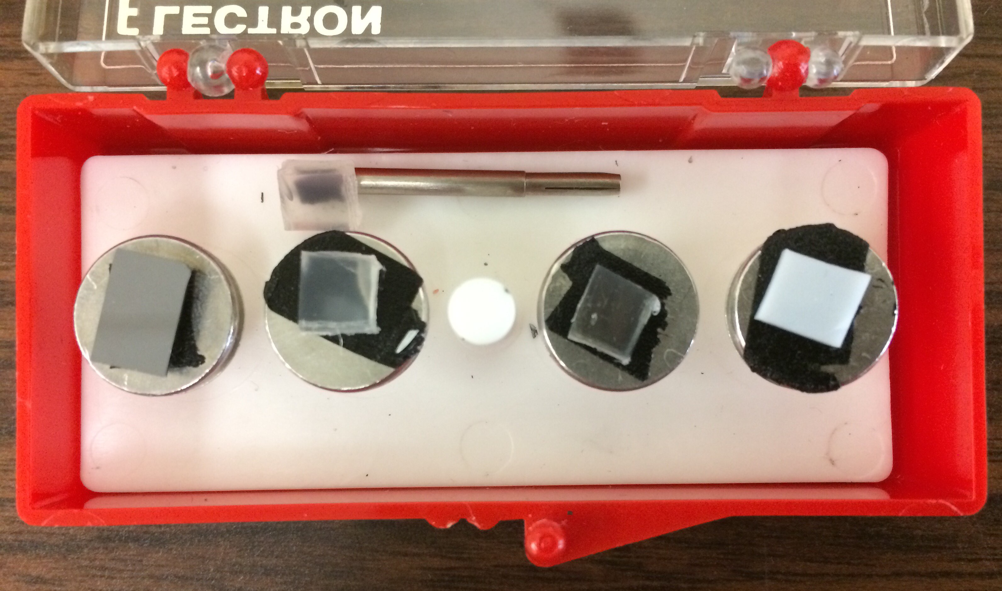
Figure 2: Sample mirrors mounted on stubs and the micromanipulator probe. Unpolished CB mirror (top, micromanipulator); (left to right) InAs mirror, polished CB mirror, metal-coated CB mirror, and Teflon mirror.
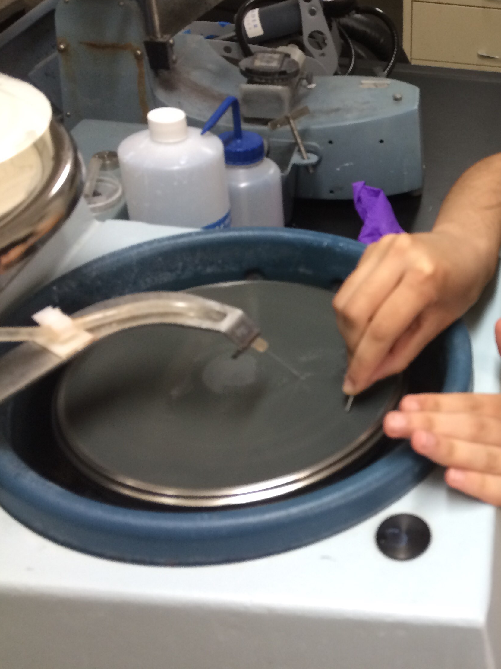
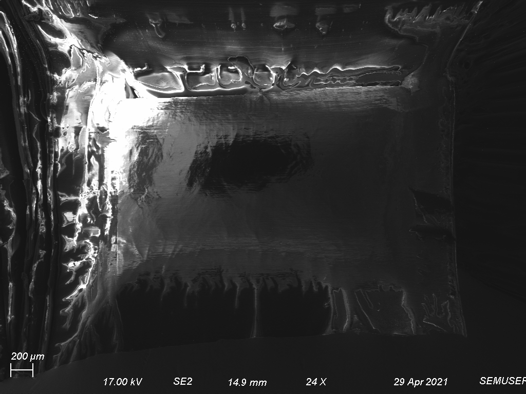
Pieces from a plastic semiconductor sample holder were cut into small squares: one was left alone, another was polished in an attempt to make its surface smoother, and a third piece was sputter coated with platinum to create a metallic surface mirror. These pieces were affectionately dubbed "Chonky Bois" due to their relative thickness compared to other mirror samples, and will henceforth be abbreviated as "CB." The semi-insulating sample was a rectangular piece of InAs wafer that was cleaved using a diamond scribe. A Teflon disk was cut into a small square piece as well. As is described in the Results and Discussion section, from these materials a most effective mirror was chosen to be mounted on the micromanipulator.
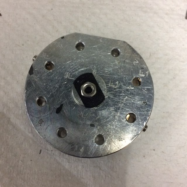
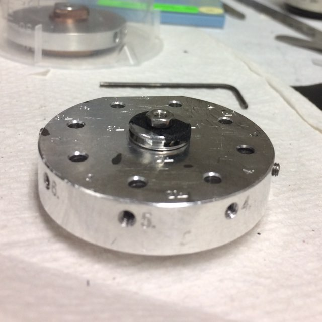
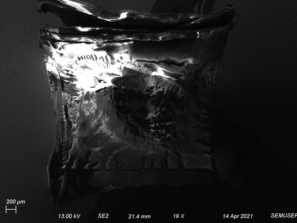
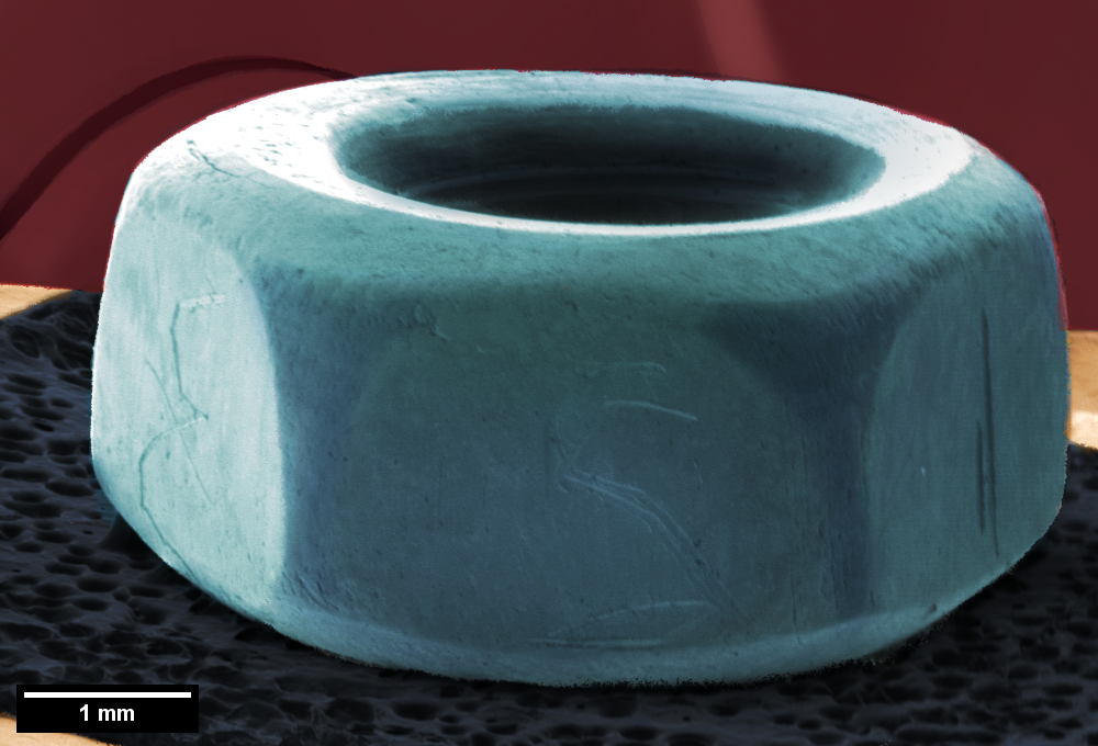
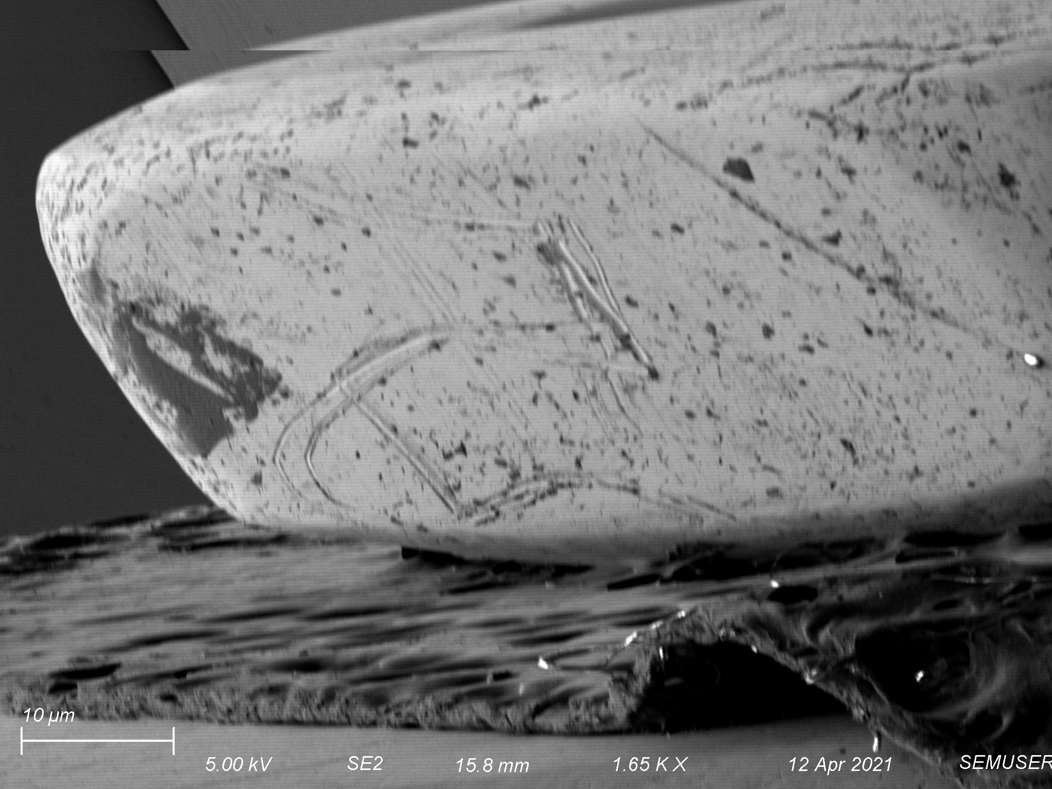
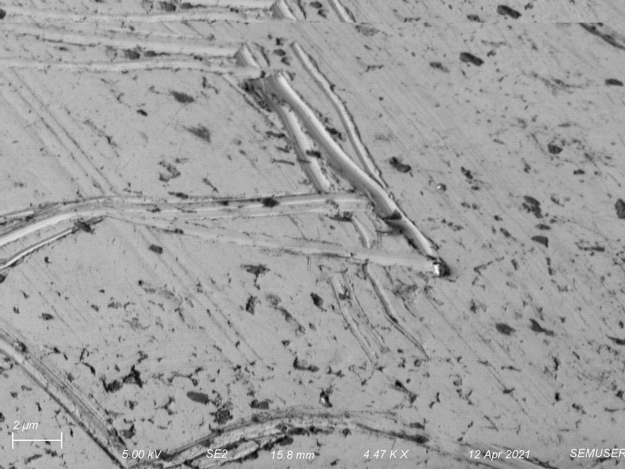
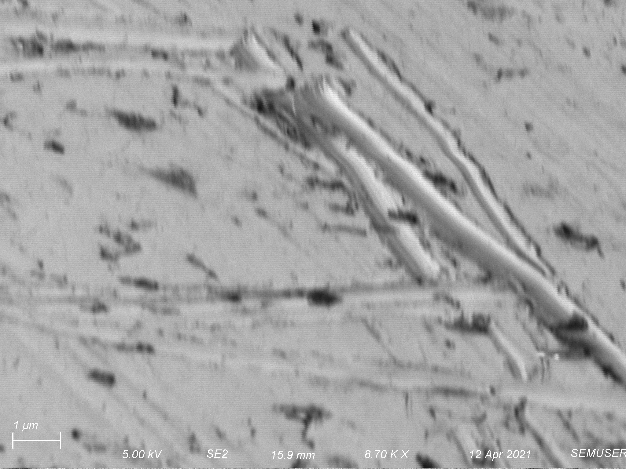
The sample imaged during this exercise was a small screw nut with the numbers 1-6 etched into each of its sides.
Figure 3: The screw nut mounted on the sample stage.
2. Charging the Mirrors
The method for charging the mirror is rather straightforward, and followed that which was described by Croccolo [5]. Once the mirror was inserted into the chamber (either mounted on the sample stage or on the micromanipulator), the SE2 detector was used to image the surface of the mirror and bring it into view of the electron beam. The magnification was increased such that only the mirror was in view of the full frame of the image, the aperture diameter was opened to 120 μm, and the beam was driven at 20 kV on high current mode. The focus was adjusted so that the focus working distance was longer than the actual working distance, creating a slightly defocused spot size on the mirror. Additionally, a slow raster scan was used. The mirrors were left to charge for 5 minutes, after which the aperture was closed to 30 μm and the accelerating voltage was brought down to 3 kV. When successful, the mirroring effect would begin and the sample chamber would be visible within seconds.
Figure 4: Surface of InAs mirror as it charges.
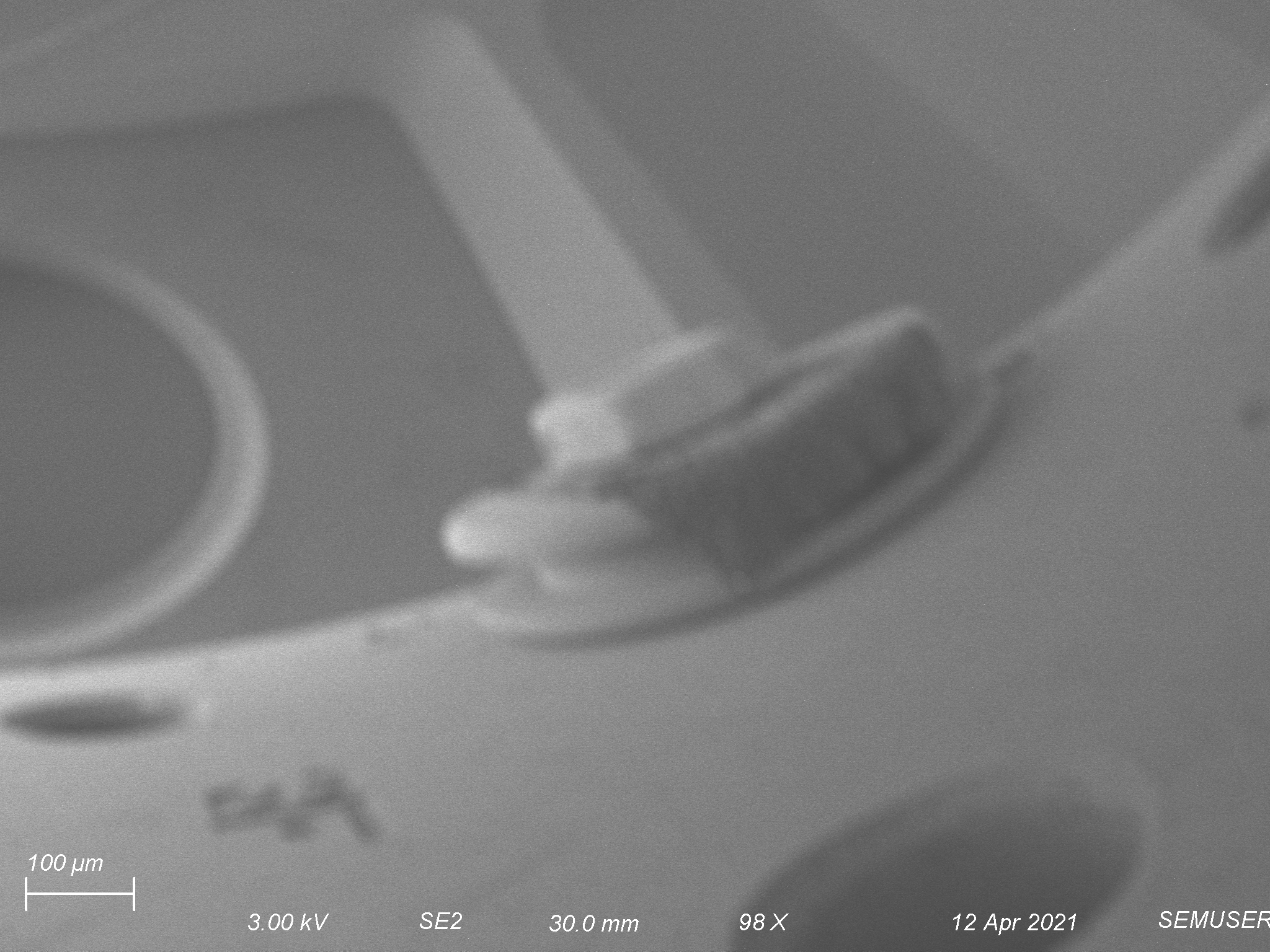
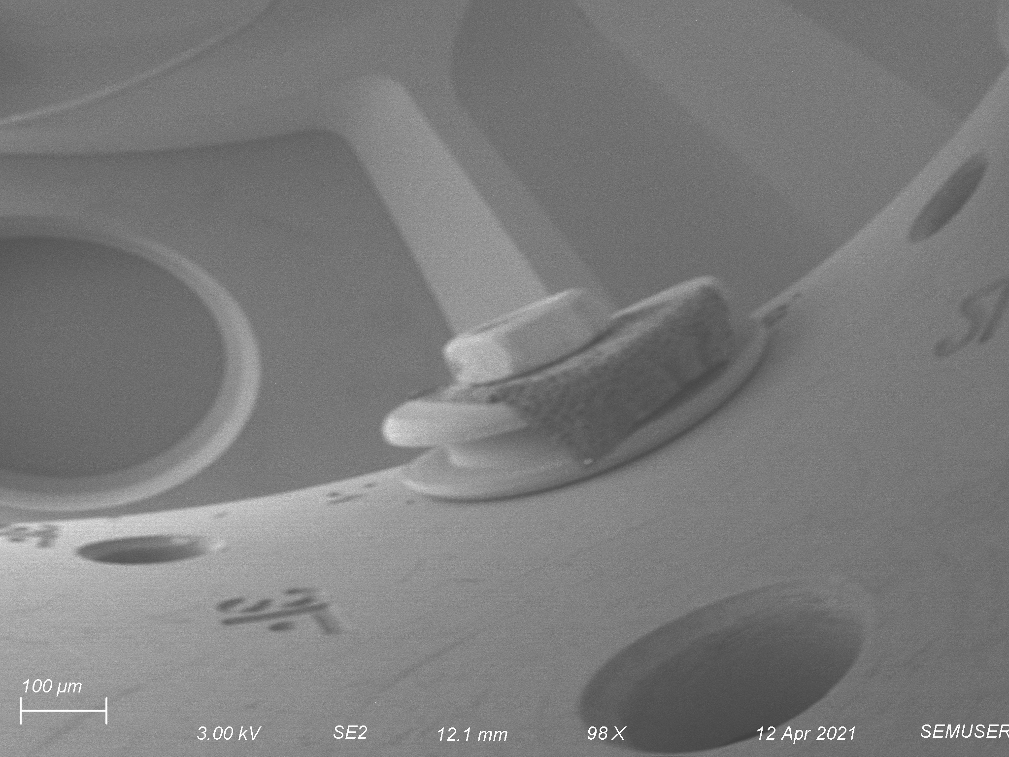
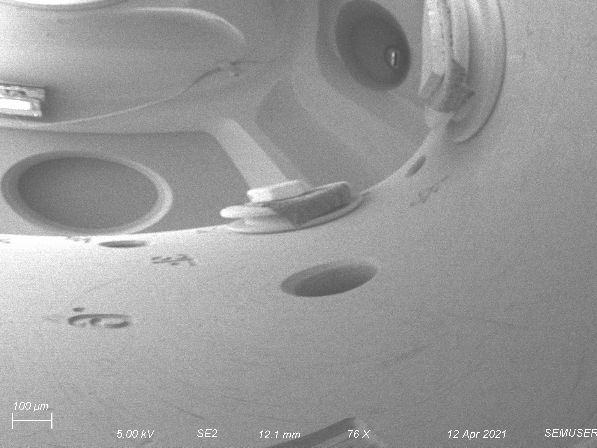
3. Mounting the Mirror on the Micromanipulator
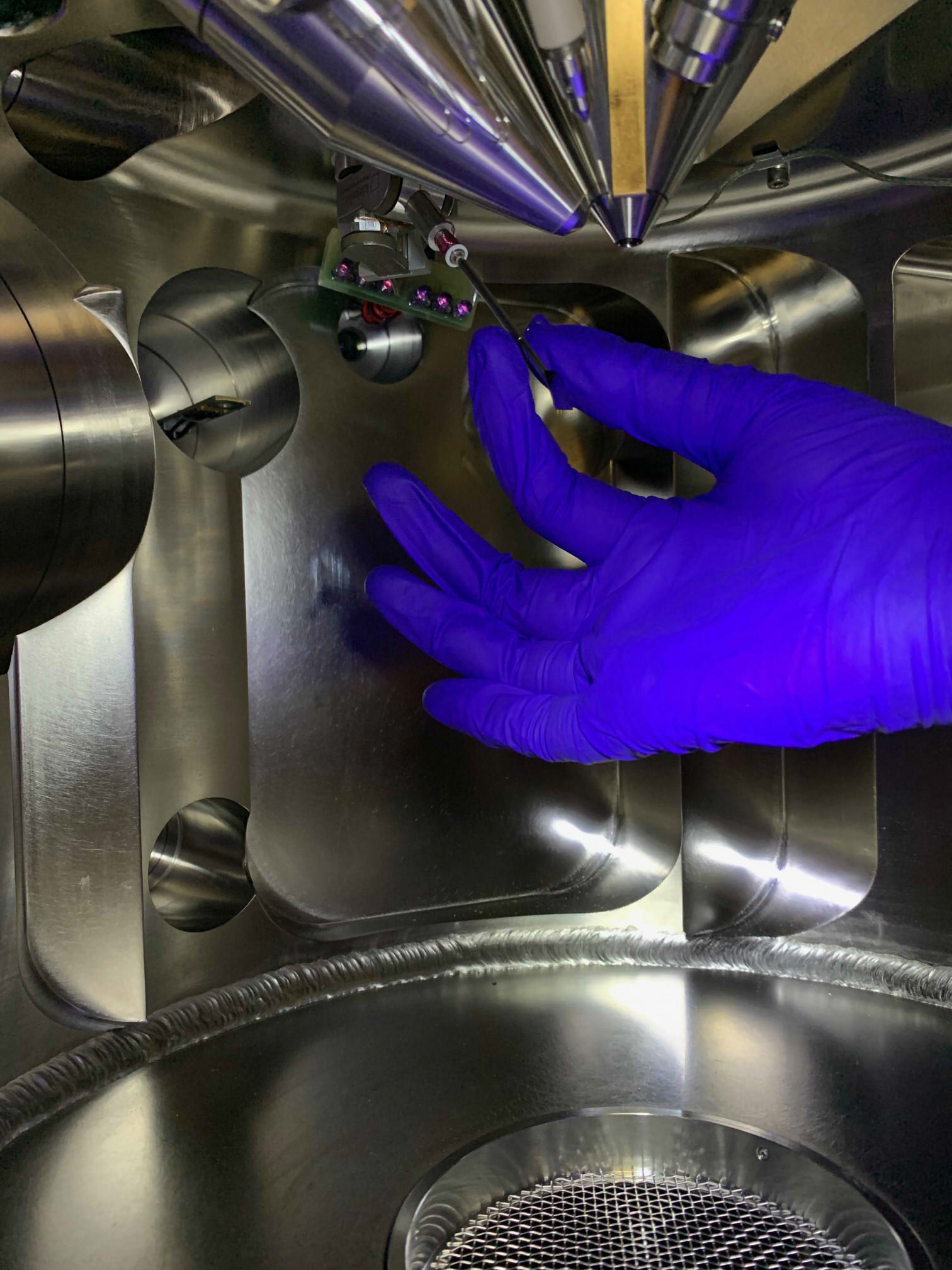
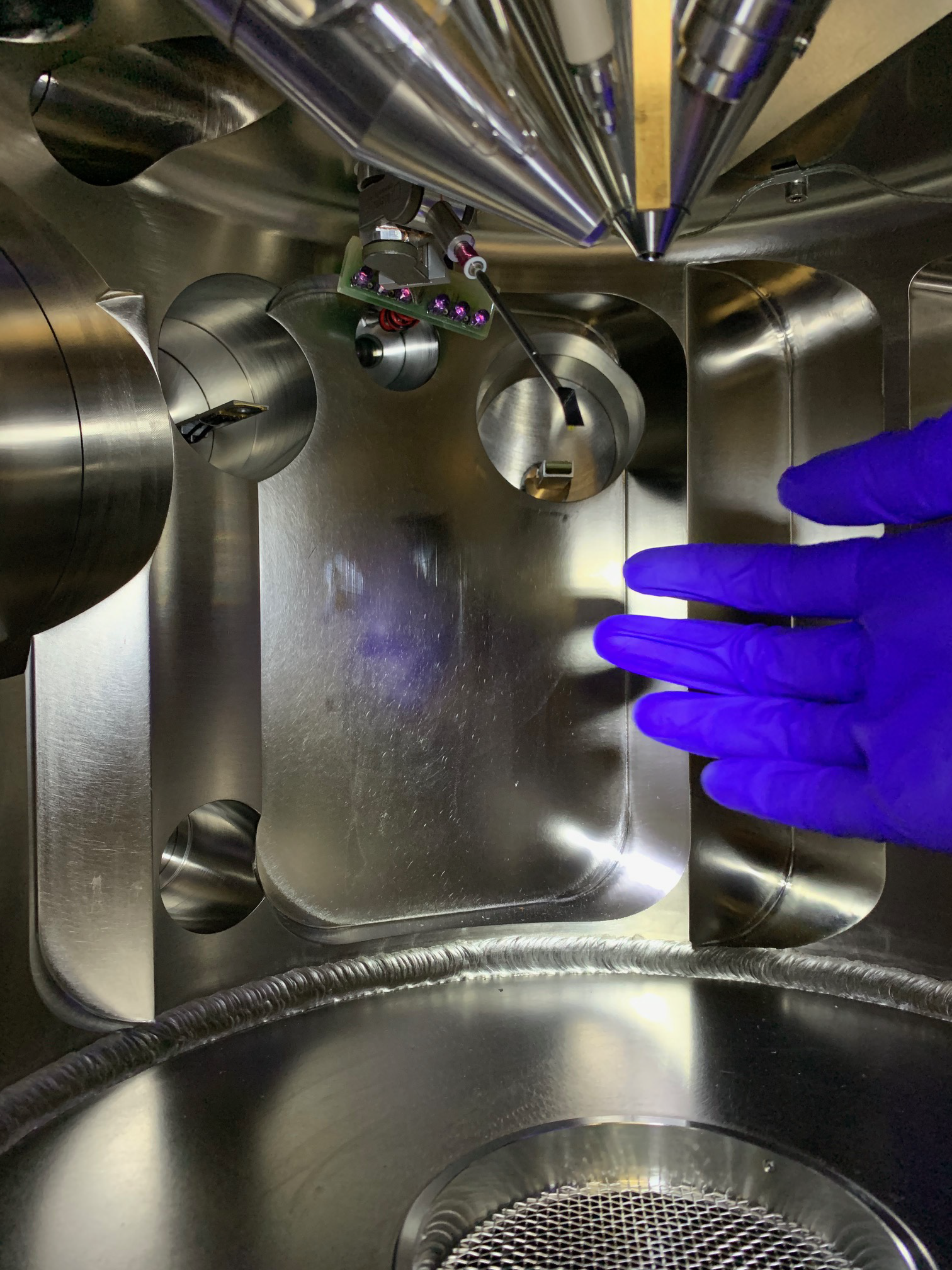
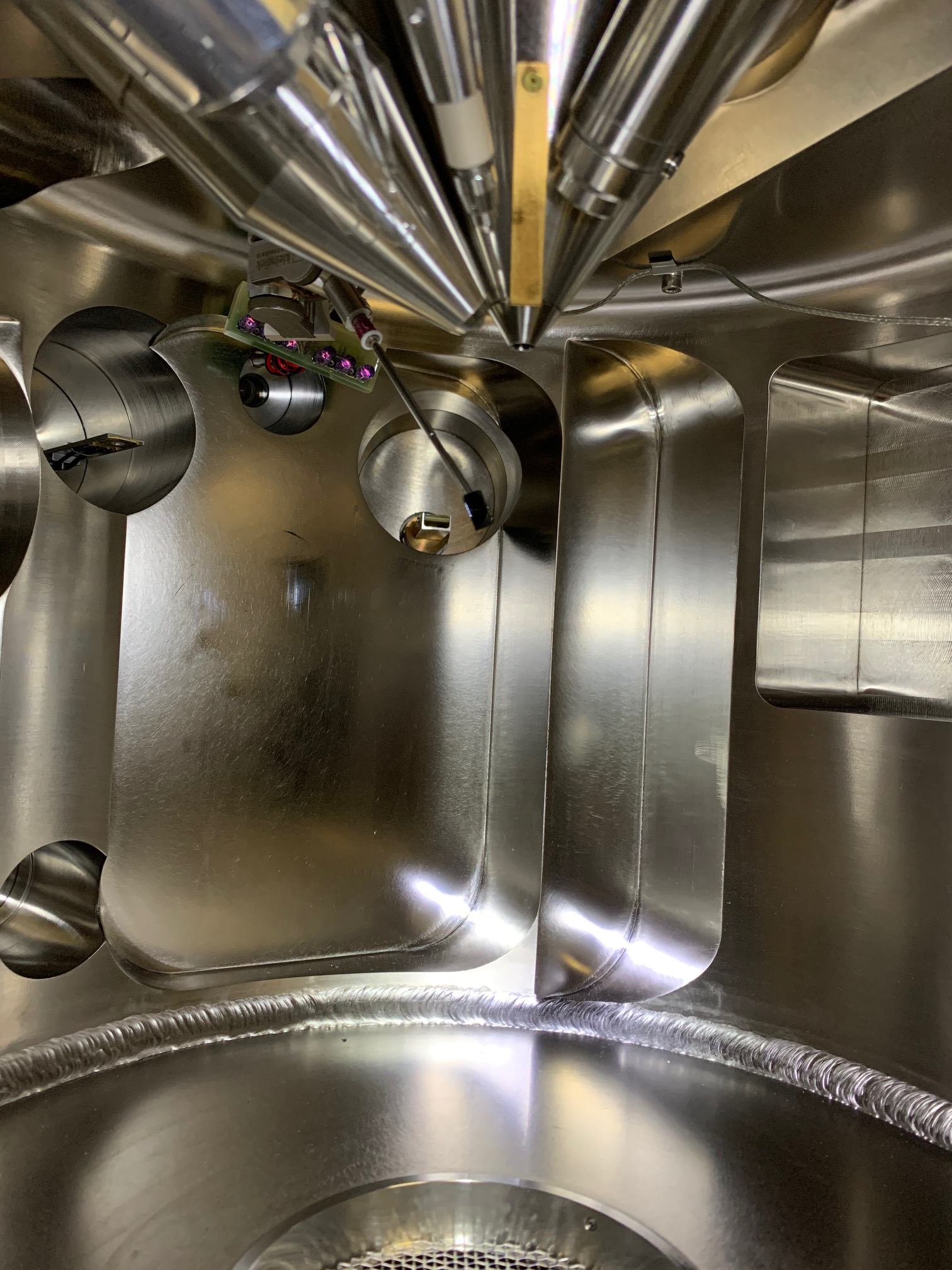
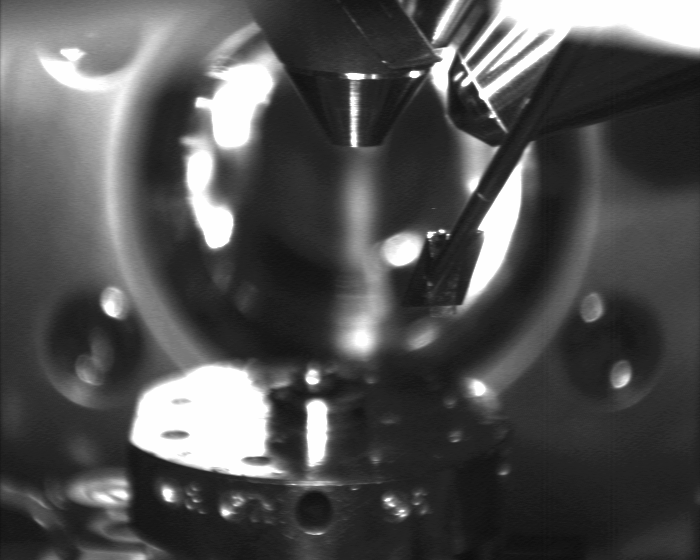
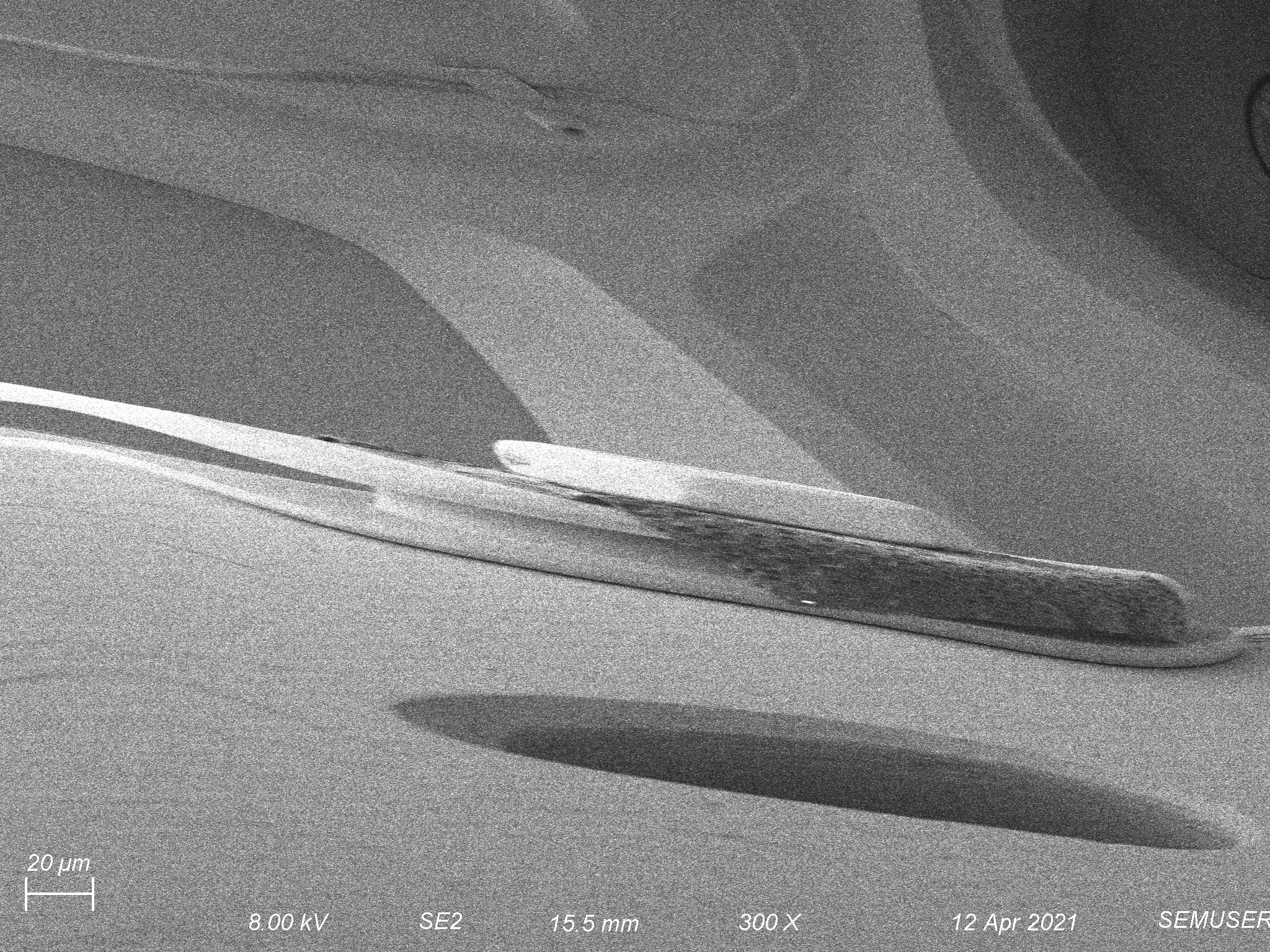
In order to manipulate the location of the mirror independently of the sample stage, the electron mirrors were mounted on a micromanipulator probe whose edge was polished down to assist in the attempt at orienting the mirror at 45 degrees relative to the incident beam. The mirror was attached to the probe with tape, and it was inserted into the micromanipulator arm within the chamber.
Figure 5: Mounting the micromanipulator probe with InAs mirror inside the SEM chamber.
Figure 6: Polishing the micromanipulator probe. An experienced eye will likely be able to tell that it is not being done well. The proper polishing was actually conducted by Brian McIntyre.
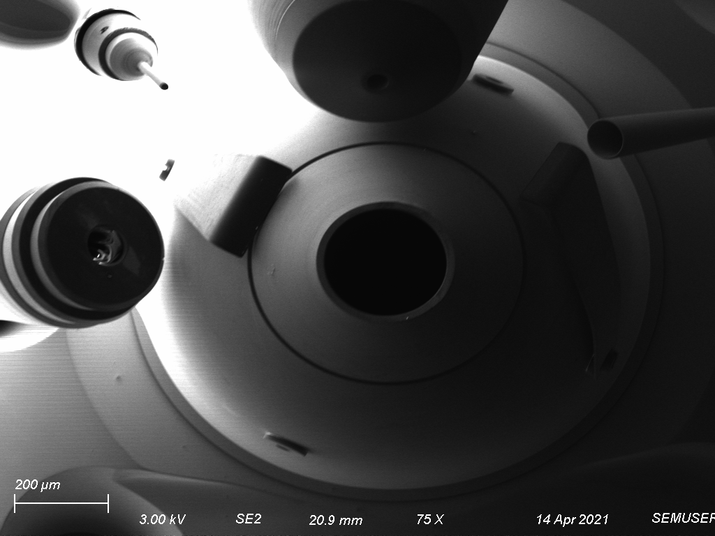
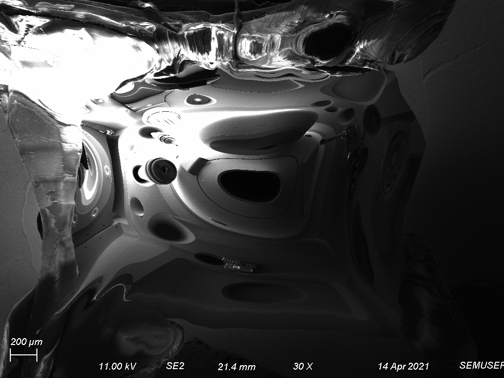
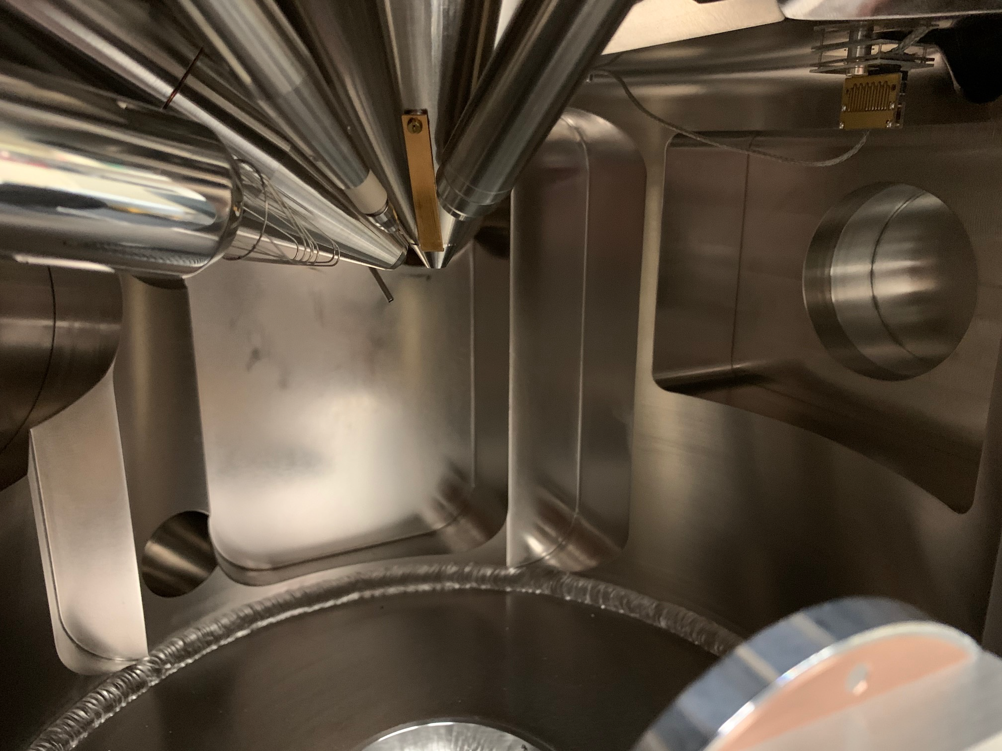
Figure 7: Camera image of the chamber interior.
Results and Discussion
1. Choosing a Mirror
Each of the mirrors were mounted on the SEM stage and inserted via load lock into the sample chamber, charged for 5 minutes each, and then the quality of their imaging was examined. The mirror quality was subjectively determined by the least amount of distortion present in the image, particularly looking for the circular shape of the final lens of the accelerating column. Additionally, the range of accelerating voltages over which the mirroring effect remained intact was examined for each material by first determining if imaging could be obtained at 3 kV, and then increasing the accelerating voltage by increments of 2 kV until the mirror crashed out.
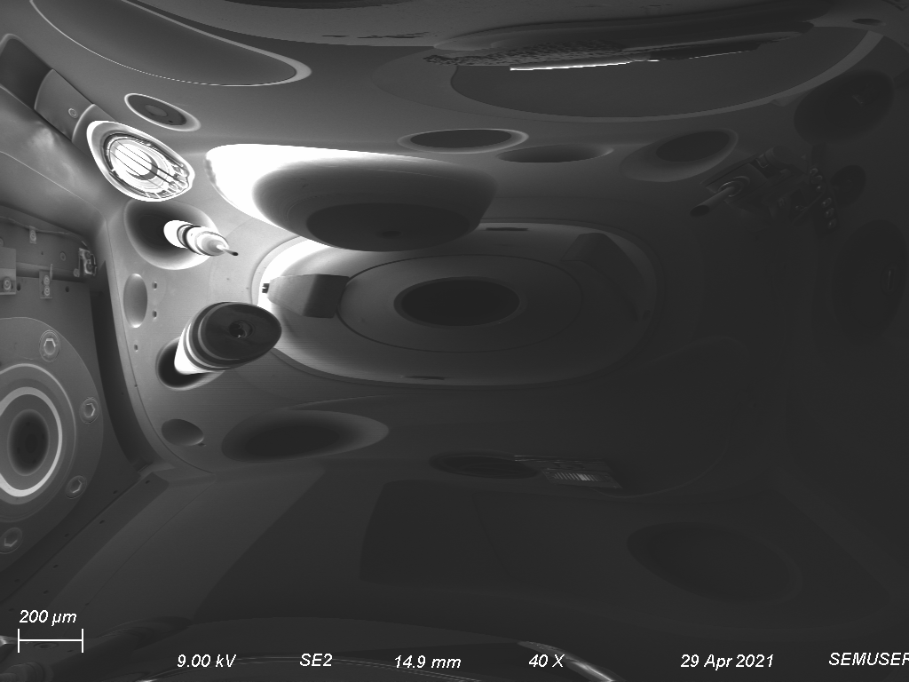
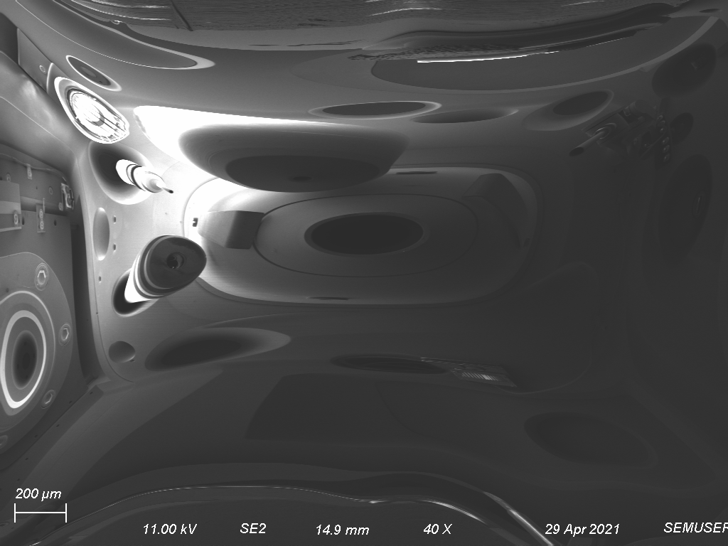
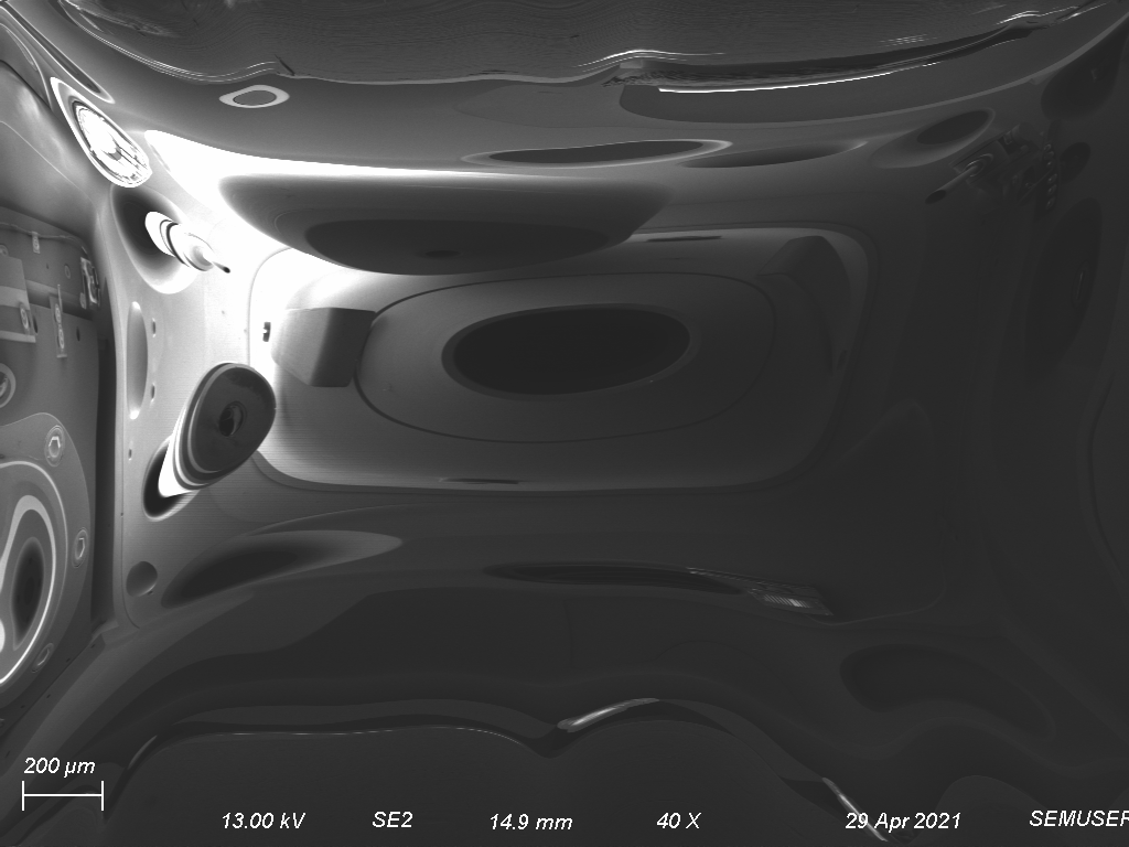
Figure 8: Plain CB mirror piece 1, before being polished from 3 kV (top left) to 13 kV (bottom right).
Figure 9: Plain CB mirror piece from 3 kV (top left) to 17 kV (bottom right).
Both plain, uncoated CBs displayed the best imaging, both in the least amount of distortion present and in the highest accelerating voltage for which the mirror remained intact. The distortion becomes increasingly more pervasive and skews te shape of the chamber as the accelerating voltage is increased. It is notable that there appears to be an apparent localization of charge on the surface of the CBs especially in Fig. 8, which contributes to the shape of the distortion of the image as it will morph to fit within this shape of localized charge. This shape is especially noticeable when the mirror is pushed to its limiting imaging voltage. The charge localization is theorized to be due to the insulating nature of plastic, which may not be allowing the charge to evenly distribute across the entire surface of the CB samples, or it could also be present due to the surface of the plastic piece not being perfectly flat and smooth. Similarly, however, it is suspected that because the CBs are insulating that this allows for a faster potential buildup on the surface and therefore causes the mirror effect to work more strongly compared to metallic or semi-insulating samples, at least with the charging conditions described in the Experimental Methods section. Although the plastic piece in Fig. 8 contains the least distortion at 3 kV (determined because the final lens exhibits the most circular shape of all the images), the plastic piece in Fig. 9 appears to have a better distribution of charge across the surface and the pattern of the distortion seems to be more predictable. In the former, the distortion takes on a sort of skewed, asymmetric shape where the image begins to be pulled into the upper right corner. In the latter, the distortion appears to be pincushion-like, stretches out more symmetrically, and the final lens takes on an increasingly rectangular shape.
Figure 10: Teflon mirror from 3 kV (top left) to 11 kV (bottom right).
The Teflon mirror displayed best highest range after the uncoated CB mirrors, imaging from 3 kV to 11 kV. However, the distortion was much more noticeably invasive. Compared to the CB mirrors, the Teflon images displayed a sort of diagonal distortion, and as the accelerating voltage increased the image of the chamber began to collapse into that diagonal. It also displayed an asymmetrical pinching — similar to that of the first CB mirror — towards the upper left corner of the image. It is unknown what about the CB mirror makes the distortion less invasive than the Teflon mirror, however examining the 11 kV image in Fig. 10 and comparing it to the 15 kV image in Fig. 9 may suggest that it has to do with the localization of charge on the surface. The Teflon surface appears rougher than the CB surface, which may explain why the charge localizes like this. For now, this mirror was set aside.
Figure 11: InAs mirror at 3 kV.
The InAs mirror was only able to image at 3 kV, as the mirror crashed out at 5 kV. The image displays a sort of pincushion distortion, which may be in part due to the rectangular shape of the semiconductor piece. The final lens displays a sort of stretching out along a major axis, and begins to look more rectangular than the expected circular shape. It was suspected that the charge would distribute more evenly across the surface of the semiconductor due to its extreme surface smoothness, however the mirror does not appear to be effective enough to consider surface smoothness as a factor here. It is possible that the InAs mirror may need extremely long charging times in order to successfully saturate the surface with enough high energy electrons, but for the scope of this project it was set aside.
Imaging could not be obtained from the metal-coated CB mirror due to unknown reasons. It was suspected that a path to ground from the surface of the mirror to the metal probe may have been created due to an unsuccessful attempt at obscuring the sides of the mirror during the sputter coating process, however this is unlikely as characteristic effects of charging were observed throughout the entire 5 minutes of charge time. Again, for the scope of this project, this mirror was set aside, although further analysis is needed to definitively determine why this mirror could not work.
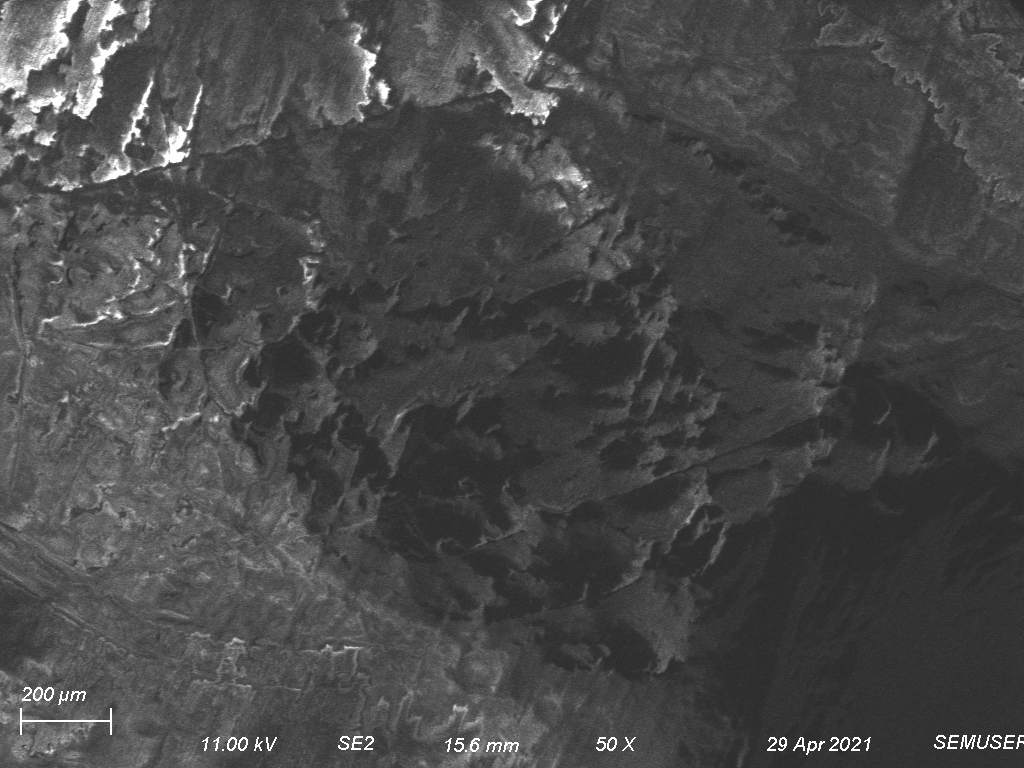
It should also be noted that a longer charging time (10 minutes) was tested out for one plain CB mirror, the InAs mirror, and the metal-coated CB mirror. It appeared to have an adverse effect on the mirrors; still no imaging could be obtained for the metal-coated CB, the InAs mirror was able to image at 3 kV but was not stable enough to last more than a minute, and the plain CB piece displayed extra noise in the imaging with faster raster scan rates (see Fig. 12) but the same range of accelerating voltages for which imaging could be observed.
Figure 12: 5 minute charge, fast scan (left); 10 minute charge, fast scan (middle); 10 minute charge, slow scan (right)
Ultimately the unpolished, plain CB was chosen as the best mirror because it was able to achieve imaging at the highest accelerating voltage. Imaging was also conducted with the polished piece, although it was not polished very well so its effectiveness is likely not as good as it could be. It is suspected that a properly smooth, polished surface may produce even better results.
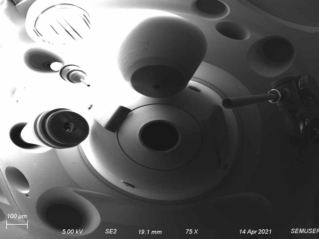
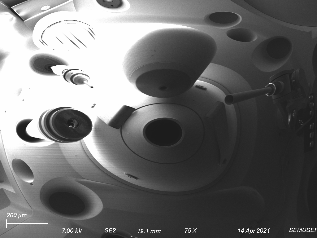
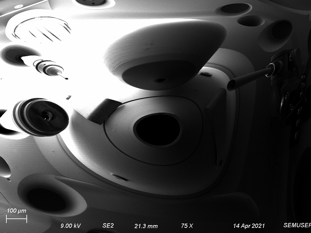
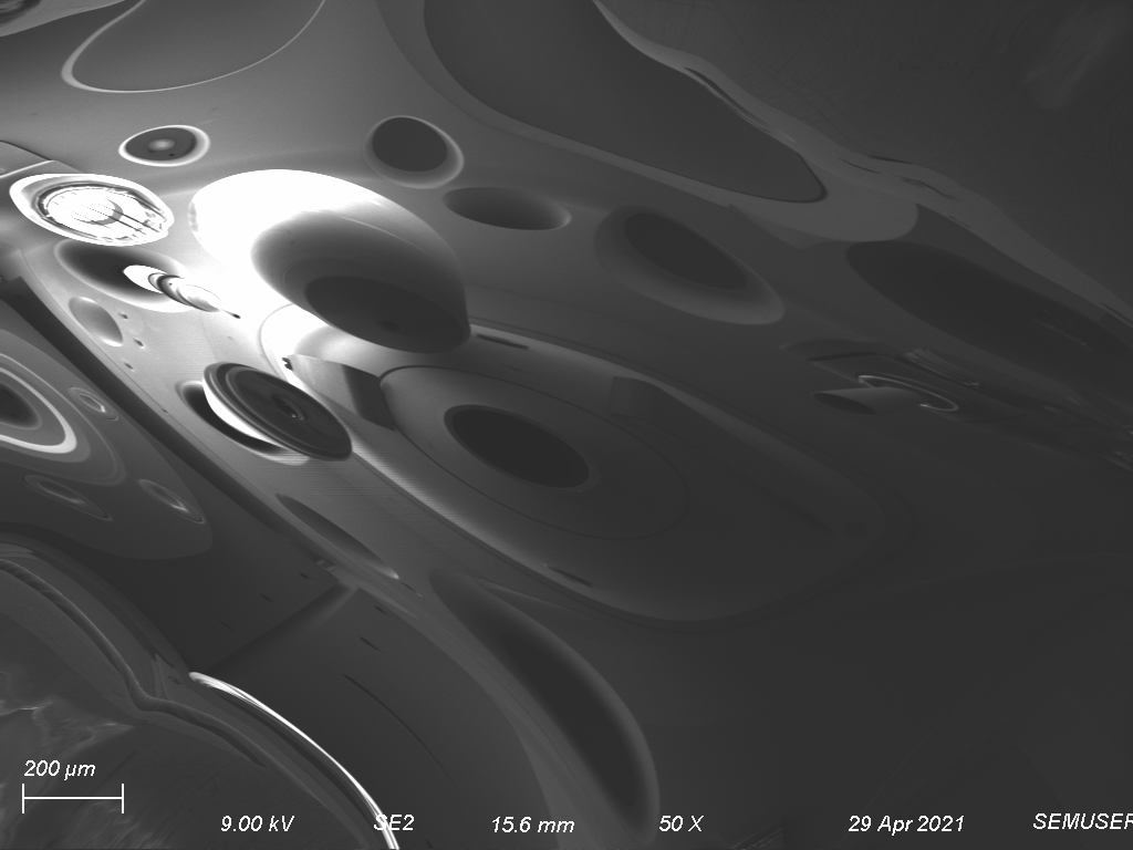
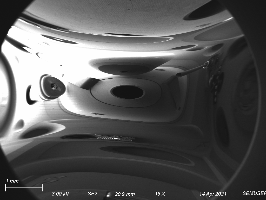
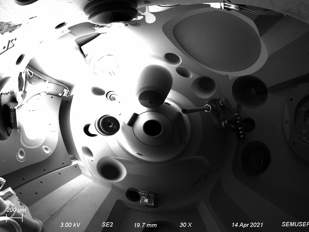
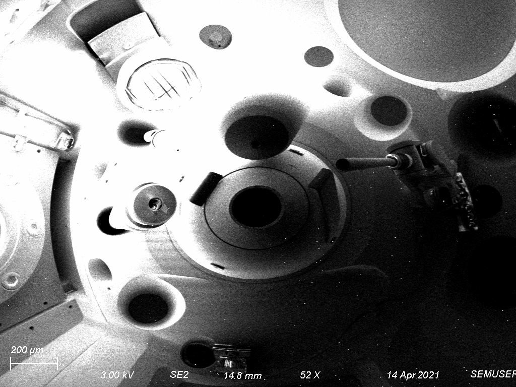
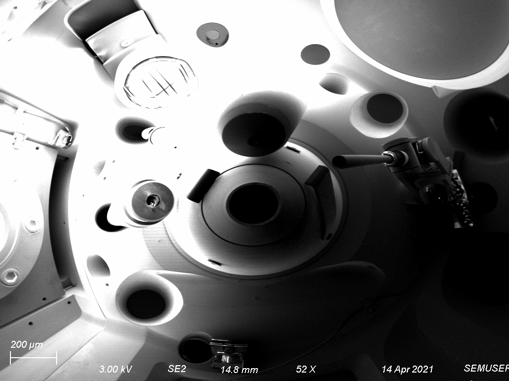
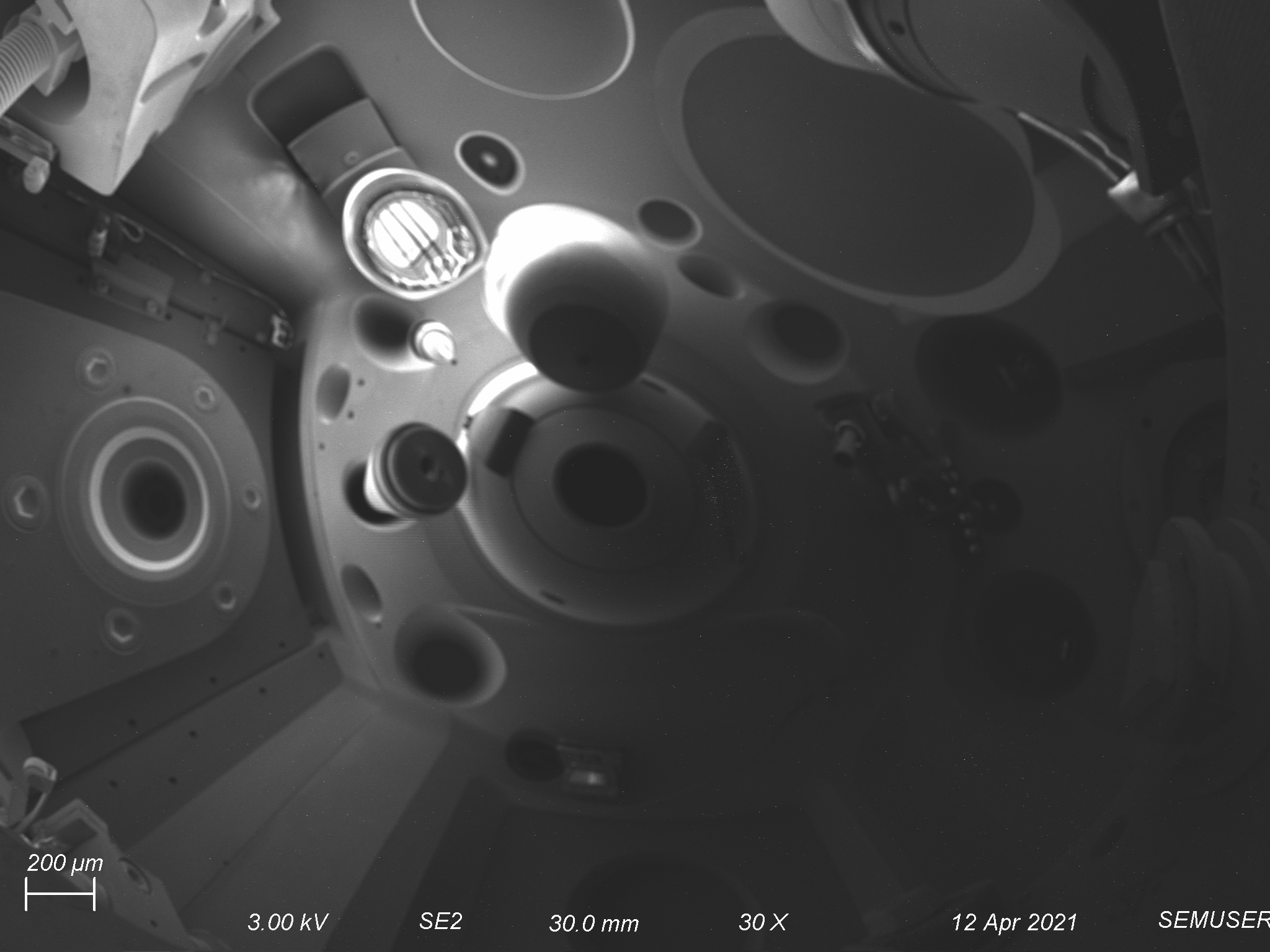
2. The Interior of the Chamber
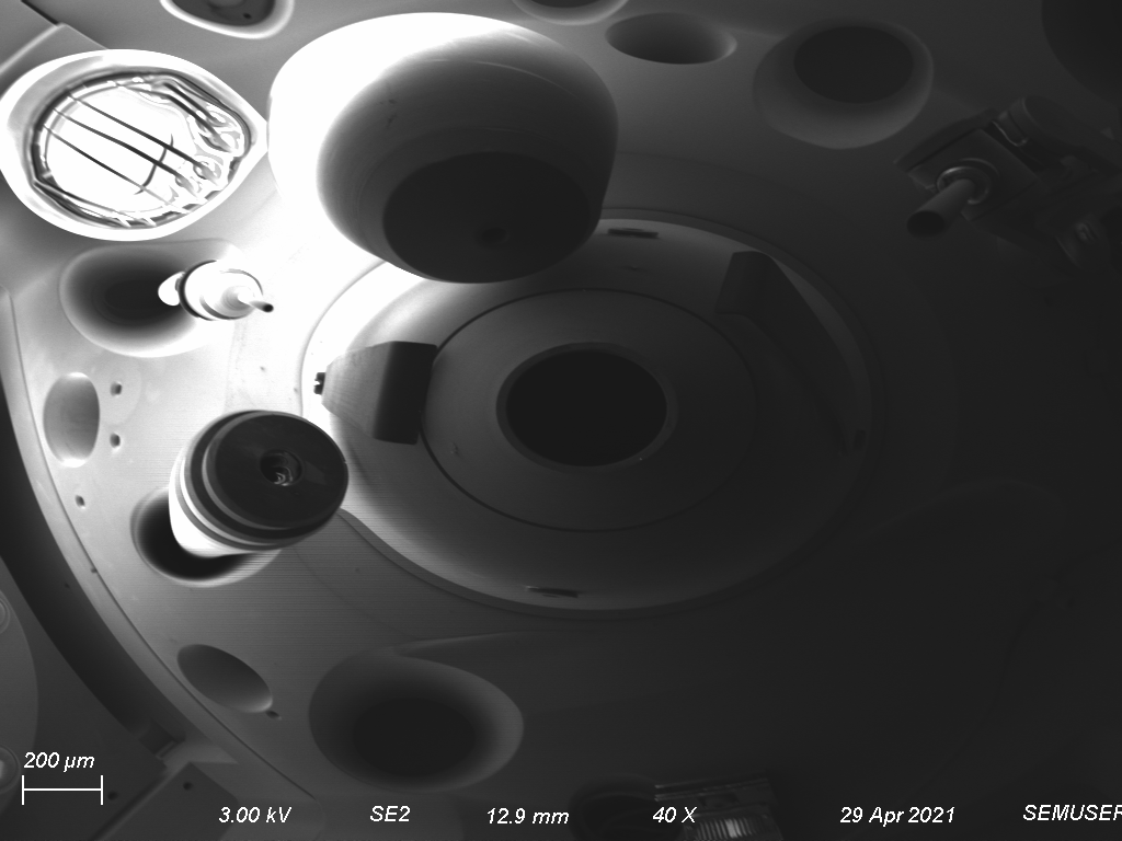
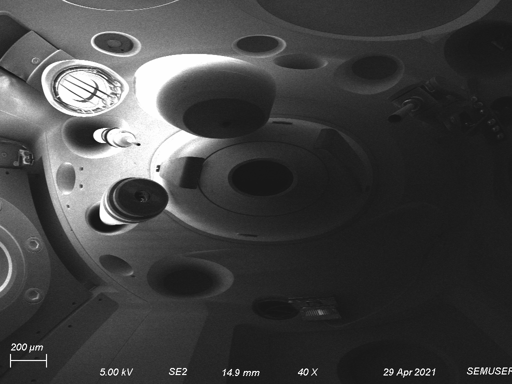
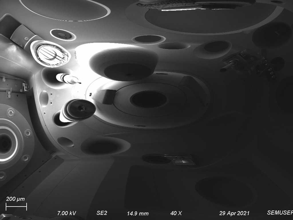
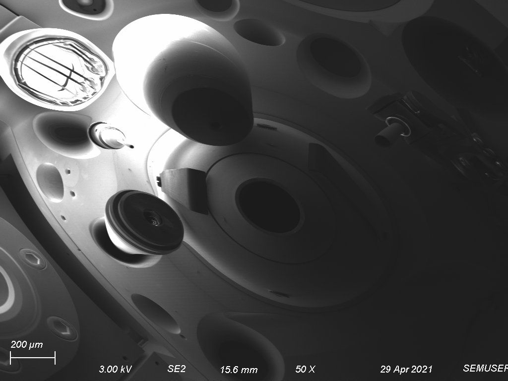
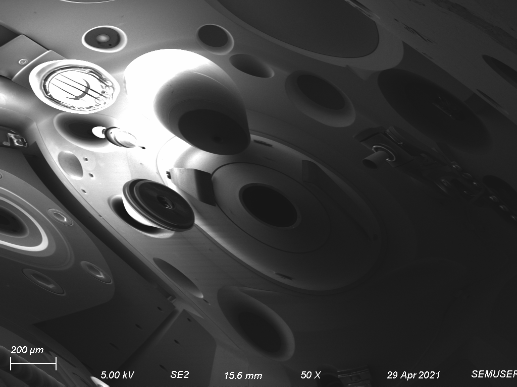
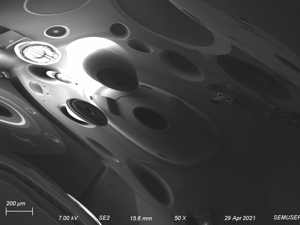
When the mirror is mounted on the sample stage and the mirror action begins, the sample chamber can be observed in real time from the perspective of the sample. This makes it a fascinating tool to use to diagnose the functionality of some of the components (as was demonstrated with the Backscatter and InLens detectors, see [3][4]).
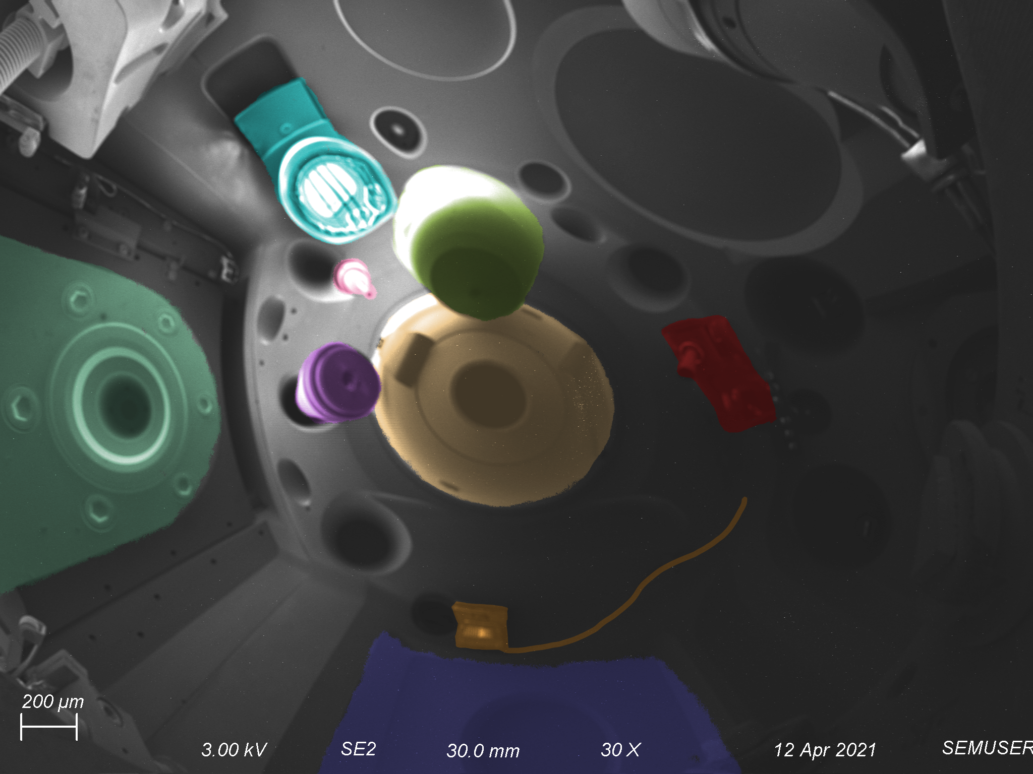
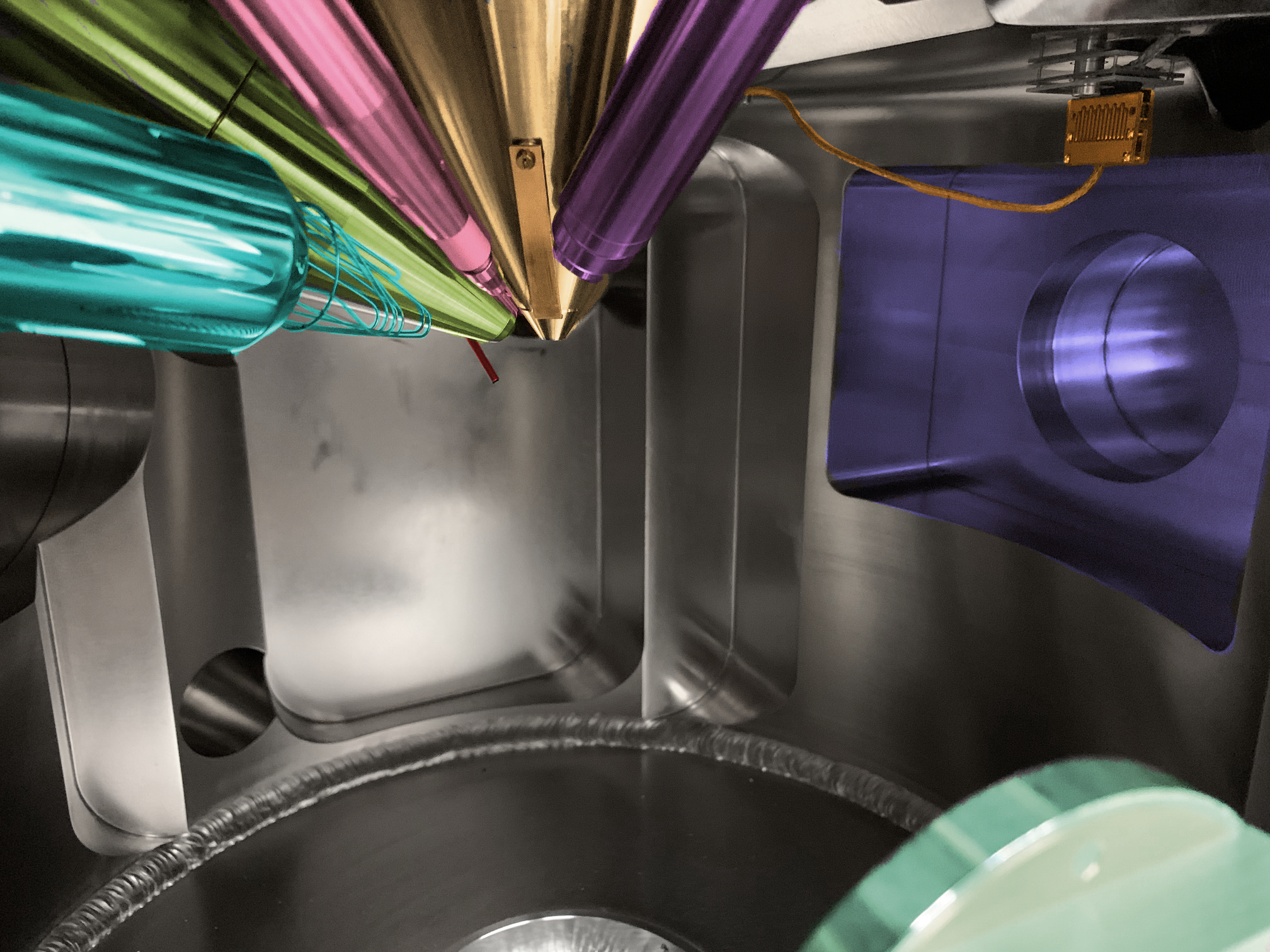
Figure 13: Images of the interior of the SEM. The leftmost images were taken from the electron mirror, while the rightmost images were taken with a phone camera while the sample chamber was vented. The bottom two images are colour-coded; the colours correspond to matching components between images.
The interior of the microscope sample chamber is displayed in Fig. 13, with the images on the left having been obtained from an electron mirror and the images on the right taken from a phone camera. The colour-coding between the bottom two images identifies matching components between the two perspectives. We will pay special attention to three of them: the final lens of the accelerating column (yellow), the SE2 detector (cyan), and the micromanipulator arm (red).
From the electron mirror images, the bottom of the final lens appears larger than it actually is because this region of the cone is closer to the mirror than the portion at the top of the chamber. Additionally, one may notice that the least amount of distortion appears to be present in the region directly above the mirror used to collect the image; this is not the final lens itself in this case, since the mirror was not located in the centre of the chamber, however noticing the deviation in the shape of the final lens from the expected circular shape can help us characterize the distortion of the mirror.
Notice that the brightest area is the SE2 detector; this is because the highest signal of secondary electrons is centred on this detector, since this is the detector used to collect the image. The location of the detector used to image an electron micrograph will act as an apparent light source for the image, which is why the SE2 detector itself almost looks like a lightbulb from the perspective of the mirror. Regions of the chamber opposite to the SE2 detector will appear in shadow because the least amount of signal is obtained from this region.
Finally, directing our attention to the micromanipulator arm, this is where the electron mirrors were later mounted. The micromanipulator can be moved on polar axes to direct the view of the electron mirrors.
Figure 14: Colourized image of screw nut imaged with unpolished CB mirror at 3 kV. The scale bar was recalibrated with the diameter of the screw nut in ImageJ.
The above, digitally colourized image was obtained with the unpolished, plain CB mirror at an imaging voltage of 3 kV. The advantage of using the micromanipulator arm allows for the potential to find a geometry within the sample chamber that produces the least distortion by moving the sample stage relative to the mirror mounted on the micromanipulator. The micromanipulator itself can be reoriented to adjust the relative angle of the mirror to the electron beam. Ideally, the mirror would be mounted at a 45-degree angle relative to the beam in order to produce a 90-degree reflection and therefore the least pervasive astigmatism in the beam, since the beam is intercepted and reflected before it is focused onto the sample. Knowing this, the working distance reported by the SEM is also incorrect, and must be recalibrated. Due to the heavy amount of distortion across the entire mirror image, however, this can only be done in small regions directly in front of the mirror, if the distortion is appropriately corrected. This was done in the above image, where the scalebar was generated from calibrating the diameter width of the screw nut.
Obtaining the region of least distortion is an iterative and time consuming process. Since the micromanipulator in the SEM cannot be placed in an absolute position, the user must guess the geometry of the micromanipulator and the stage. The user can then move the sample stage to a region of least distortion, adjust focus and astigmatism, and then move the mirror again. This process is repeated until an ideal geometry is found, or until the user gets tired and accepts defeat. This is best done at lower accelerating voltages, since the distortion in the mirror image increases with accelerating voltage.
The novelty of mounting the electron mirror onto the micromanipulator is in allowing the user to use the full mobility of the stage in order to image different regions of the sample. Once a satisfactory geometry is established, the user can rotate or tilt the sample stage in order to view different orientations of the sample without the need to vent the chamber and remount/replace the sample.
Figure 15: A focused image of a "6" engraved on the sample stage.
One may point out that the numbers in Figs. 14 and 15 are mirrored. This is due to the direction of the raster scan. If the raster were instead scanned in the reverse direction, the numbers would read normally.
3. Imaging Multiple Sides of the Screw Nut
Once the mirror was mounted onto the micromanipulator probe, it was brought into the view of the frame, charged, and then the voltage was crashed down to 3 kV to begin imaging. Most imaging done with the micromanipulator was done at 3 kV or 5 kV due to the least amount of distortion present at lower voltages. A suitable geometry for which the least distortion on the screw nut could be observed was obtained through an iterative process of orienting the micromanipulator, then moving the sample stage until the sides of the screw nut were as perfectly vertical as possible. Once the distortion was sufficiently minimized, the magnification was adjusted as to only include the screw nut within the view of the frame. The stage was then set to rotate, and live videos of the rotation were recorded, as are shown in Figs. 16 and 17 below.
Figure 16: 360-degree rotation of a screw nut imaged with the unpolished, plain CB mirror at 3 kV (left) and 5 kV (right).
Figure 17: 360-degree rotation of a screw nut imaged with the polished, plain CB mirror at 3 kV.
Even though it is not guaranteed that the ideal geometry with the least distortion was obtained for each of these videos, notice that there appears to be an apparent diagonal distortion in the 5 kV video compared to the 3 kV video in Fig. 16. Additionally, Fig. 17 shows that the polished mirror (that, again, was polished rather poorly) appears to show a sort of flattening distortion of the screw nut. Still, reasonably quality videos can be obtained of the live imaging and rotation of samples with this method, and features can be resolved quite well. Not only do each of the videos show the scratched in numbers on the surface of the screw nut, as well as being able to see the grooves on the interior, but small surface roughness features are also visible.
4. Limitations to Electron Mirror Imaging
The electron mirror is an exciting and incredibly versatile tool, however it does have major limitations in its current implementations. One of its biggest limits is in the resolution of images at high magnification. Due to the poor astigmatism in the beam and the incredible depth of focus introduced from the increased working distance, it is difficult to properly bring a sample into focus at high magnification. Even when using the beam stigmators to their limits, the astigmatism still cannot be fully corrected. This causes poor focusing of samples when imaging with the electron mirrors, and is why it is crucial to obtain an appropriate geometry between the electron beam, the electron mirror, and the sample stage.
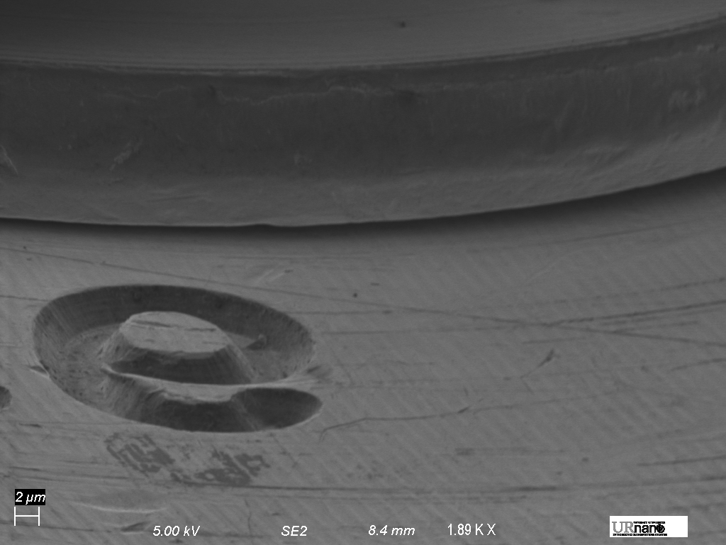
Figure 18: Imaging the "5" etched into the screw nut with the plain CB mirror at increasing magnifications at 5 kV. Notice the inability to focus the image at the highest magnification.
Obtaining the right sample geometry is not a straightforward process, however, and is severely disadvantaged by the current inability to consistently place the micromanipulator arm in the same orientation, since it is lacking in control absolute coordinates. Its polar movements (adjusting its position angularly instead of an xyz coordinate) also make it difficult to move the mirror to a different location in the chamber while maintaining the same relative angle to the electron beam. Currently, finding a region of least distortion and astigmatism is a process that can take hours.
Figure 19: Images of the screw nut obtained from the plain CB mirror: defocused at 3 kV (top left), best focus at 3 kV (top right), best focus at 5 kV (bottom left), and best focus at 8 kV (bottom right).
Distortion also proves to be a troublesome issue with electron mirrors. When attempting to image the sample chamber at higher accelerating voltages, the distortion of the image can greatly skew the shape of the sample and make it difficult to obtain useful information. It also prevents the calibration of the magnification with a known feature size, since the distortion may skew the relative sizes of different regions and directions within the sample chamber. This makes it difficult to use any numerical information provided by the SEM other than the accelerating voltage.
Ending Remarks
1. Directions for Future Work
Although successful demonstration of the electron mirror mounted separately from the sample stage was achieved, there is a breadth of further investigation and experiments where this project can lead.
Further analysis on creating the most effective mirror – from its shape to its known smoothness – is a primary source of interest. Not enough time could be dedicated within the scope of this project to thoroughly analyze the successful imaging from each mirror material or why, however further examining ultrasmooth surfaces such as semiconductor wafers, or considering insulating surfaces that were prepared through deposition methods may help in producing an even distribution of charge across the surface of the insulator, which will serve to reduce the absurd amounts of distortion present. Additionally, analyzing the relationship between mirror area and imaging quality would be another factor to explore, as well as quantitatively analyzing the optimum time to charge a mirror depending on its composition, shape, surface area, and thickness.
Additionally, establishing a method to create a reproducible geometry such that a perfect 45-degree angle can be obtained between the mirror and the electron beam (thus producing a right-angle reflection) and orienting the sample on the same plane as the mirror will be especially useful in reducing the pervasiveness of beam astigmatism, which is an apparent limit to the resolution that can be achieved at high magnification with these mirrors. Currently, there is no way to consistently quantify the orientation of the micromanipulator arm within the SEM, neither absolutely nor relative to the stage itself, which makes finding regions of least distortion and astigmatism a time-consuming and subjective iterative process.
Examining the imaging quality of the mirrors at different charging voltages is also likely to produce interesting results. For the purpose of this project, the charging voltage was fixed at 20 kV and the best mirrors tended to lose the mirroring effect at around 11 kV. Analyzing the relationship between the charging voltage and maximum imaging voltage for different mirrors and seeing if there is a benefit to charging the mirrors with significantly high accelerating voltages may prove to be informationally useful.
As the development of these electron mirrors becomes more sophisticated, developing systems for which the mirror can be independently controlled and powered may introduce an interesting set of problems to explore. For now, the proper exploration of the electron mirror is still in its earliest stages, and as such there is an open sandbox for the exploration of their capabilities, which have the potential to greatly enhance the field of electron microscopy.
2. Acknowledgements
A thorough and sincere thank you to Greg Savich and Brian McIntyre for their patience, wisdom, and enthusiasm throughout the course of this project. The results may not have been nearly as interesting without their help. Greg was especially a great help in obtaining and preparing the materials for these mirrors and was kind enough to sit through far too much time on SEM with me.
An additional thank you to Karla Rosalia Sanchez-Lievano for being an absolutely lovely TA and a delight to learn microscopy from. Many hours in front of the SEM were made engaging and fun with her guidance!
And finally, a small nod to my friend Kenyon Carlson, who listened to me ramble about my mirrors as I worked through this project. Thanks for letting me bore you.
3. References
[1] B. McIntyre. "Electron Beam Sample Interactions." OPT 307/407 Lecture, University of Rochester, Rochester, NY. April 2021.
[2] F. Croccolo, C. Riccardi. Observation of the ion-mirror effect during microscopy of insulating materials, Journal of Microscopy 229 (1), 2007.