2. Sample Preparation
2.1 Patterned Substrate
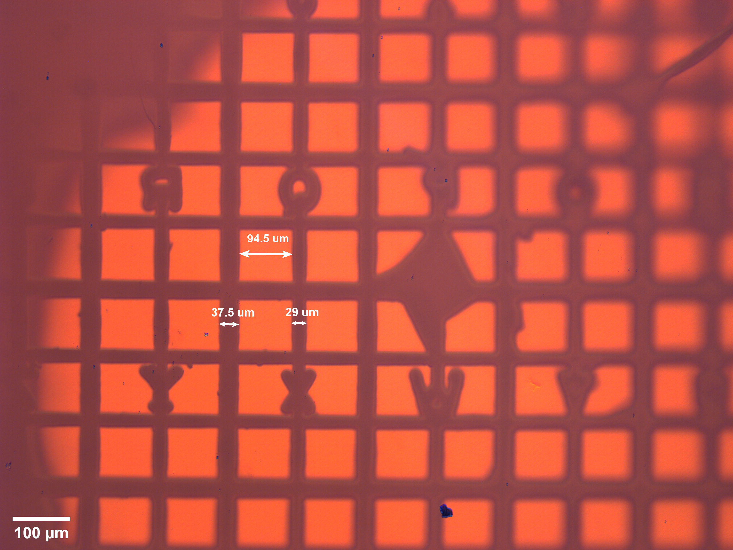
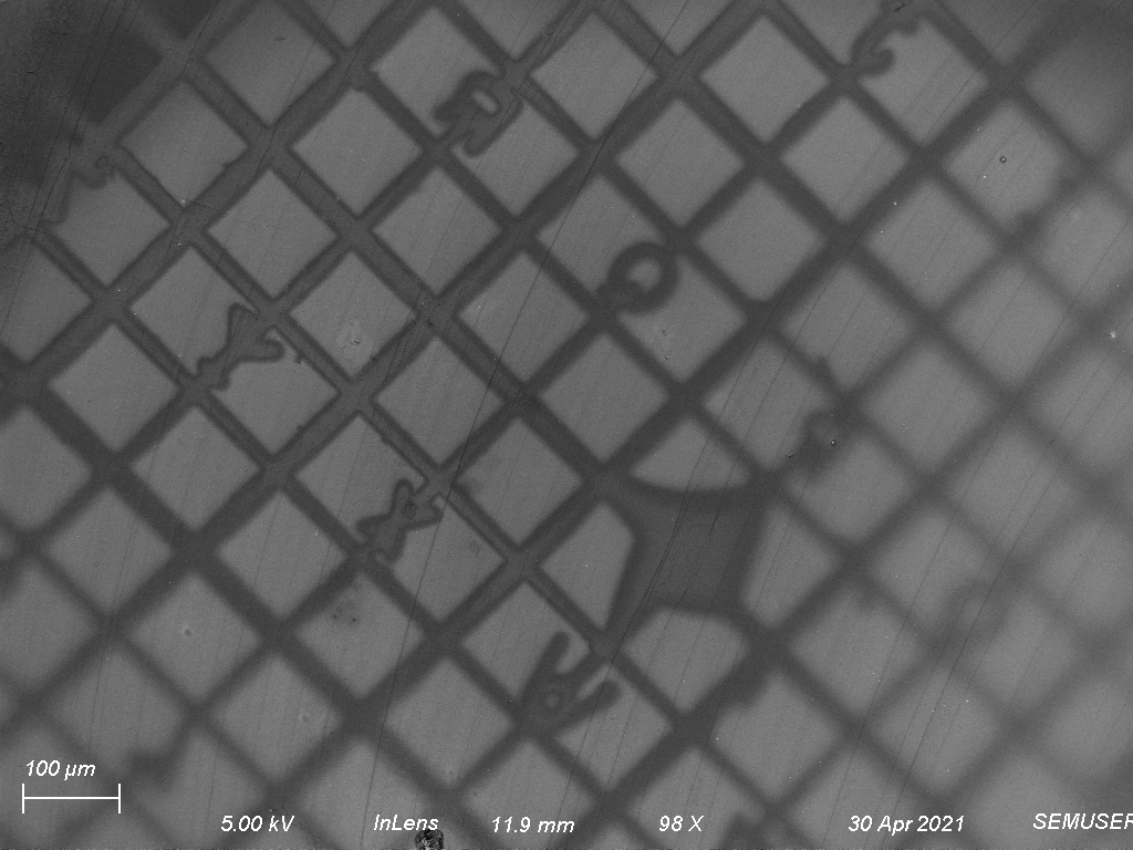 Figure 1 - Gold deposited (20 nm) onto ITO quartz coverslip using a TEM grid shadow mask. (left) Bright-field light microscope image (right) SEM micrograph
 2.2 SEM Samples
2.3 TEM Samples
3. Electron Flight Simulations
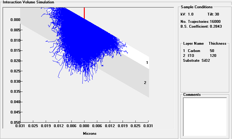
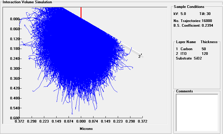
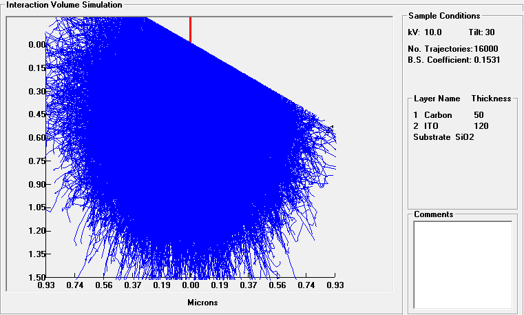 Figure 2 - Electron interaction volume simulation for ITO on quartz sample with varying beam accelerating voltages (left) 1 kV (center) 5 kV (right) 10 kV
 4. SEM Micrographs
4.1 Gold-Patterned ITO Quartz Sample
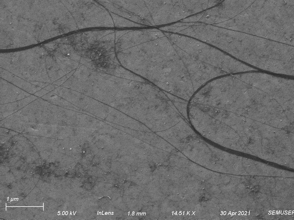
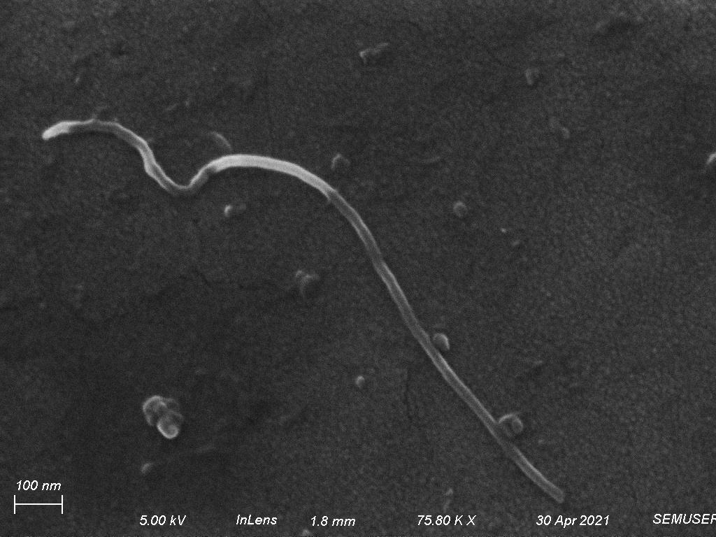
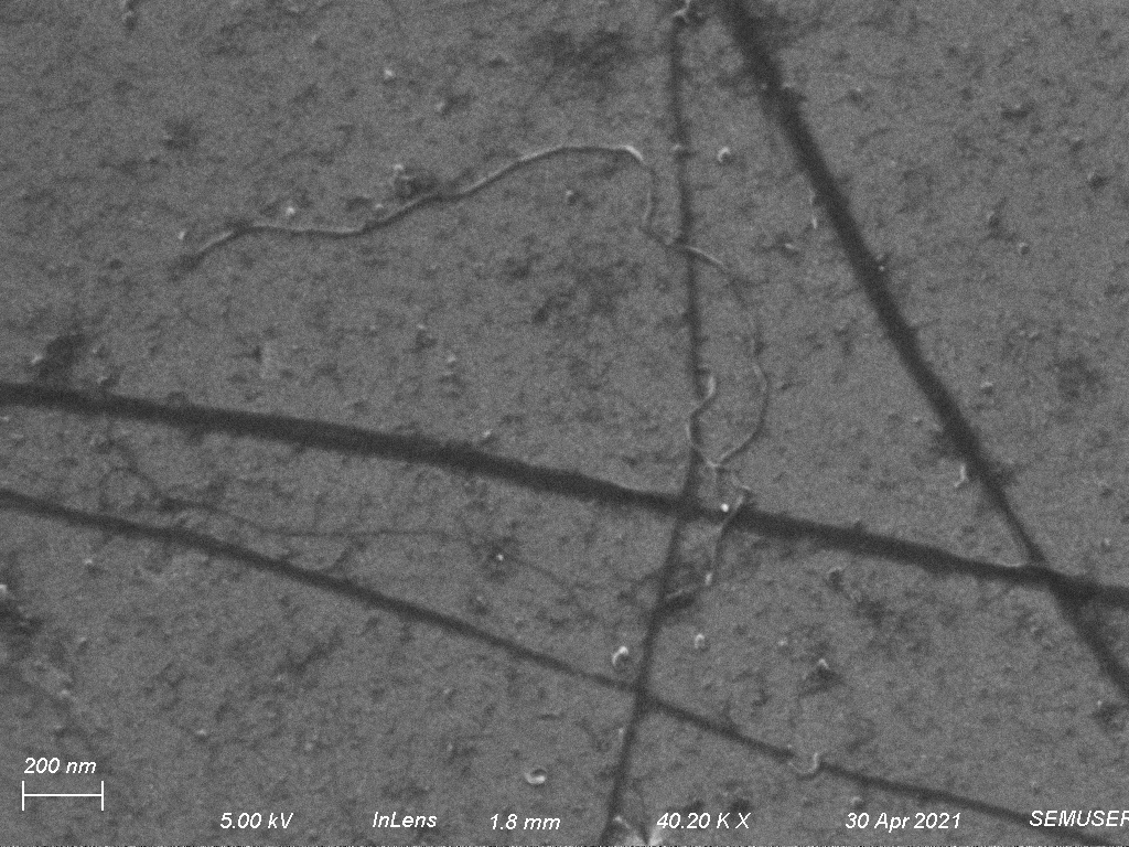
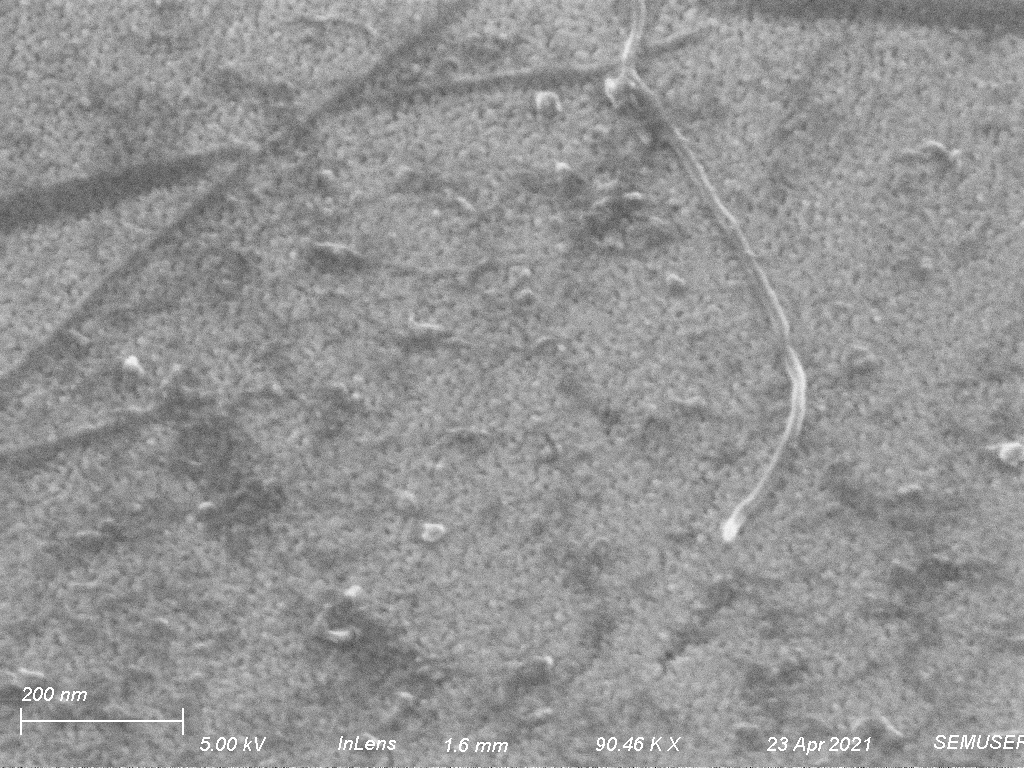 Figure 3 - SEM micrographs of NTs deposited (drop-casted) onto ITO quartz. Both long bundled and short surfactant wrapped tubes are observed with various morphologies
 4.2 Carbon-Support Film Sample
Figure 4 below shows some micrographs from the carbon support film sample and the resolution and SNR are clearly degraded compared to the ITO sample. Significant sample degradation was observed at even 1 kV and the tubes appeared to be transparent. Lowering the beam voltage to 0.5-0.6 kV reduced any raster scan artifacts but the beam was very difficult to focus at such a low voltage. This sample was also tilted at about 30 degrees relative to the beam to provide some topographic perspective. Compared to the ITO sample micrographs, we see contrast inversion as the tubes appear bright with dark background - perhaps indicating a smaller interaction volume with most of the signal arising from the tube surface. Figure on the right shows a crack in the surfactant and/or carbon film with a tube appearing to get stretched over the trench. This maybe a single tube or perhaps the surfactant on the tube getting extended as the sample was drying. Nominal individual tube diameters are expected to be around 3-5 um for surfactant covered tubes, however these SEM micrographs clearly show larger sizes - which will be analyzed in the AFM section.
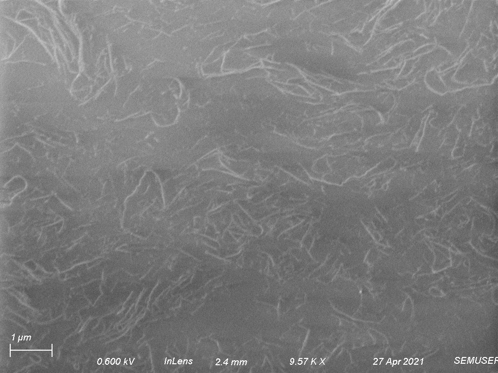
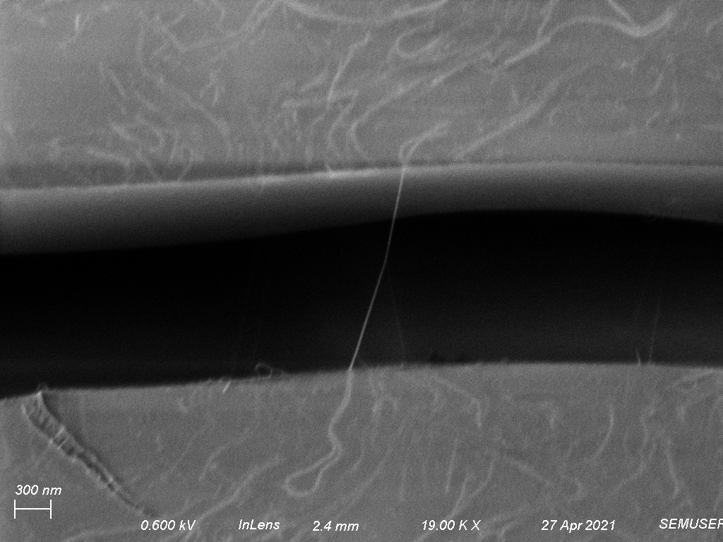 Figure 4 - SEM micrographs of NTs deposited (drop-casted) onto carbon support film (TEM grid) taken at low 0.5 kV.
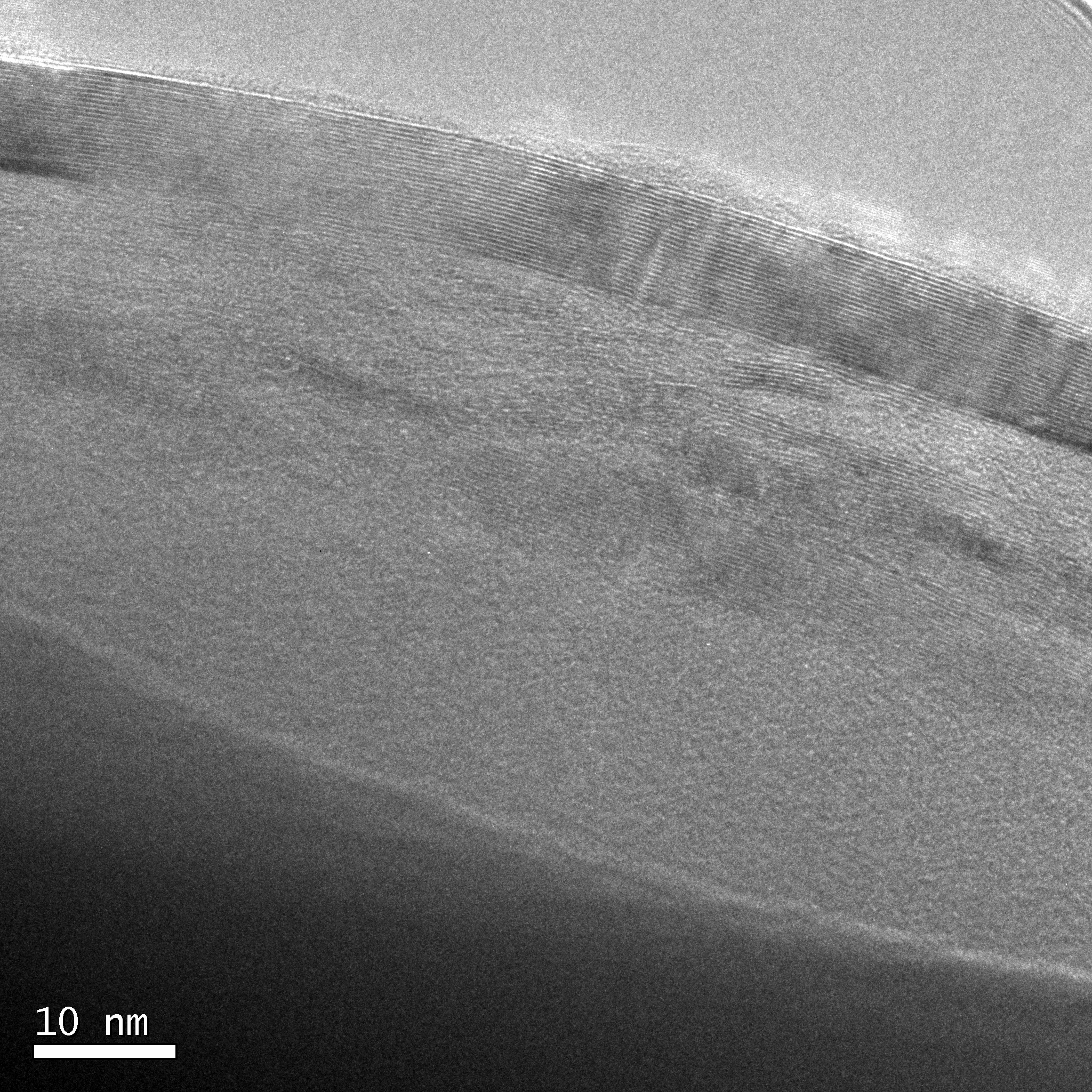
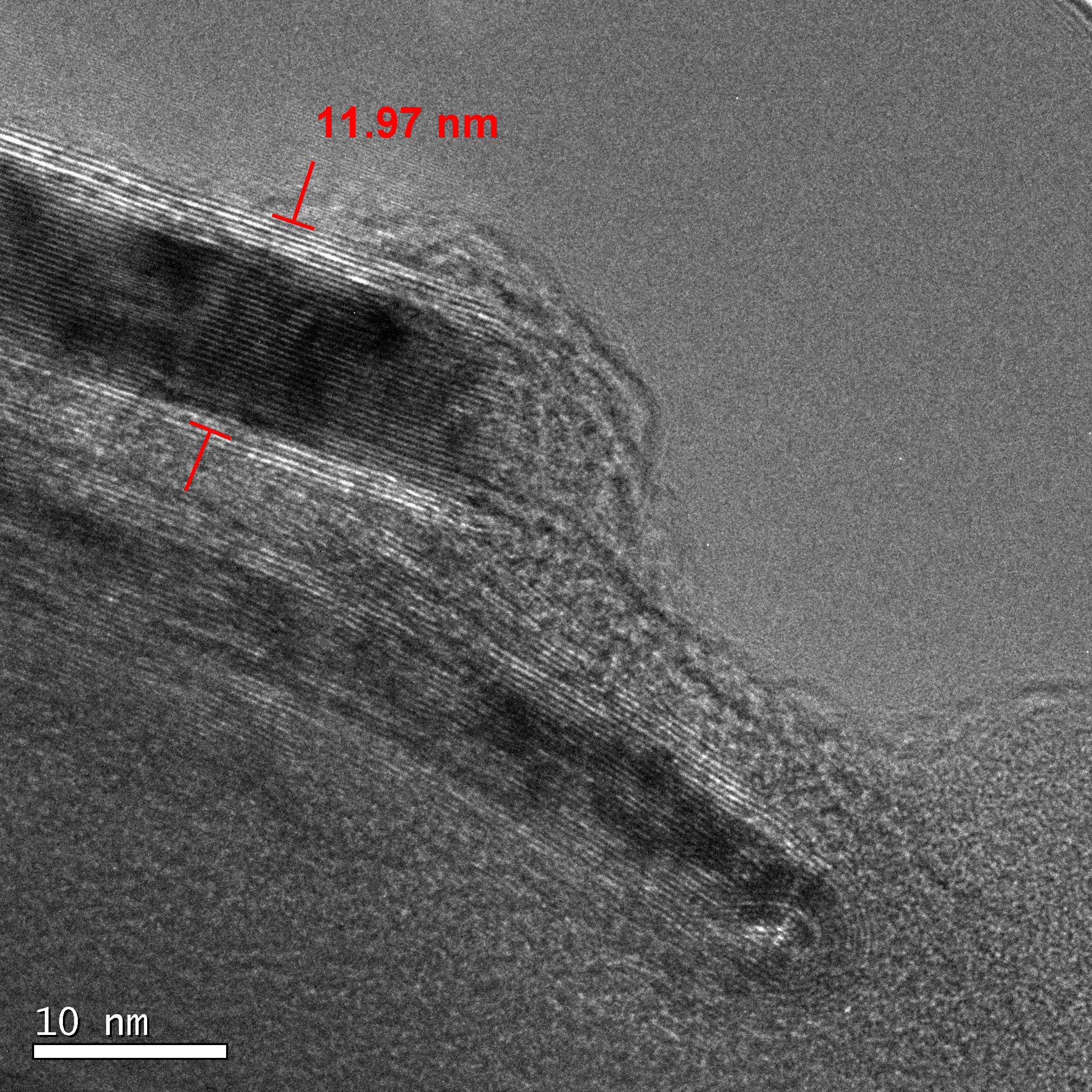
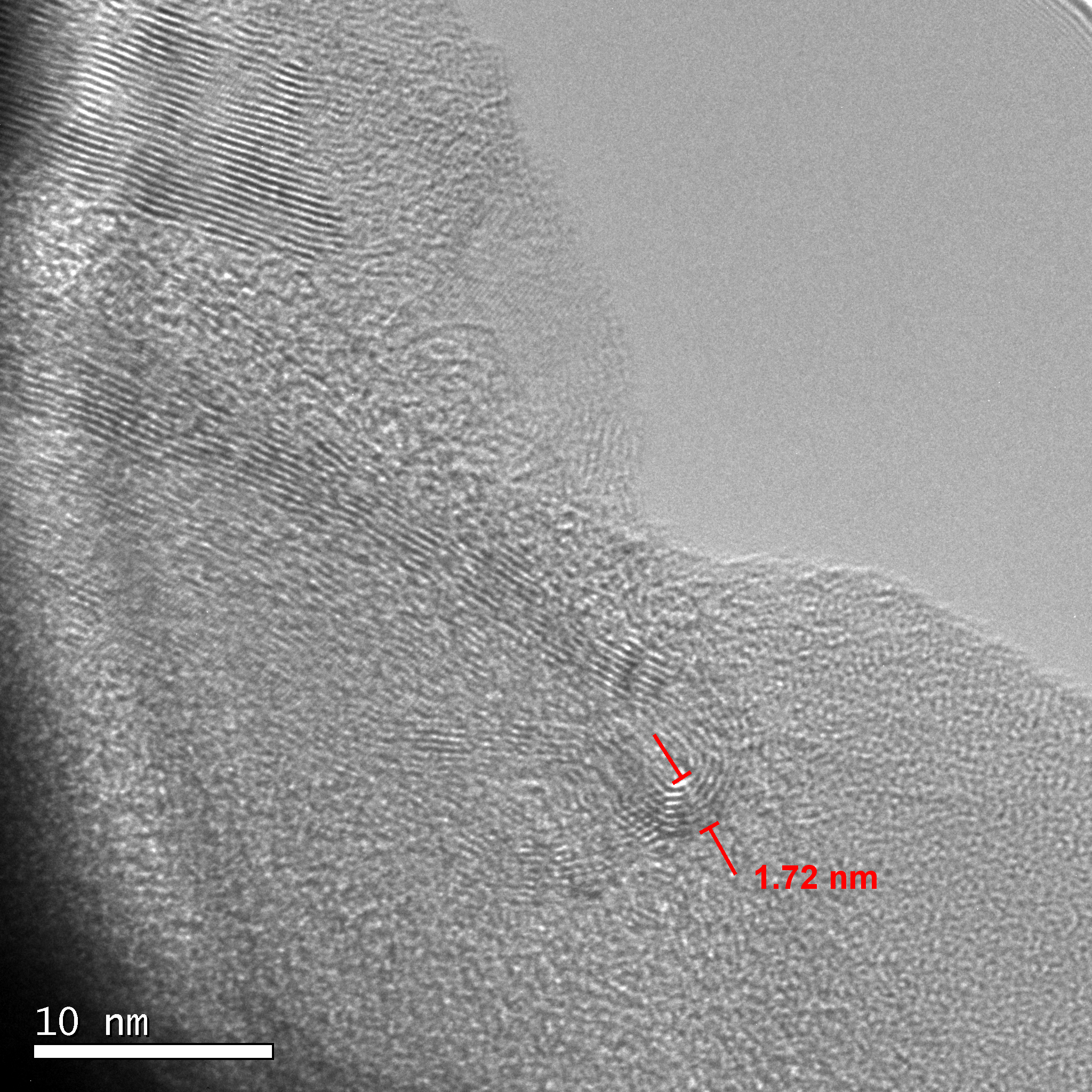
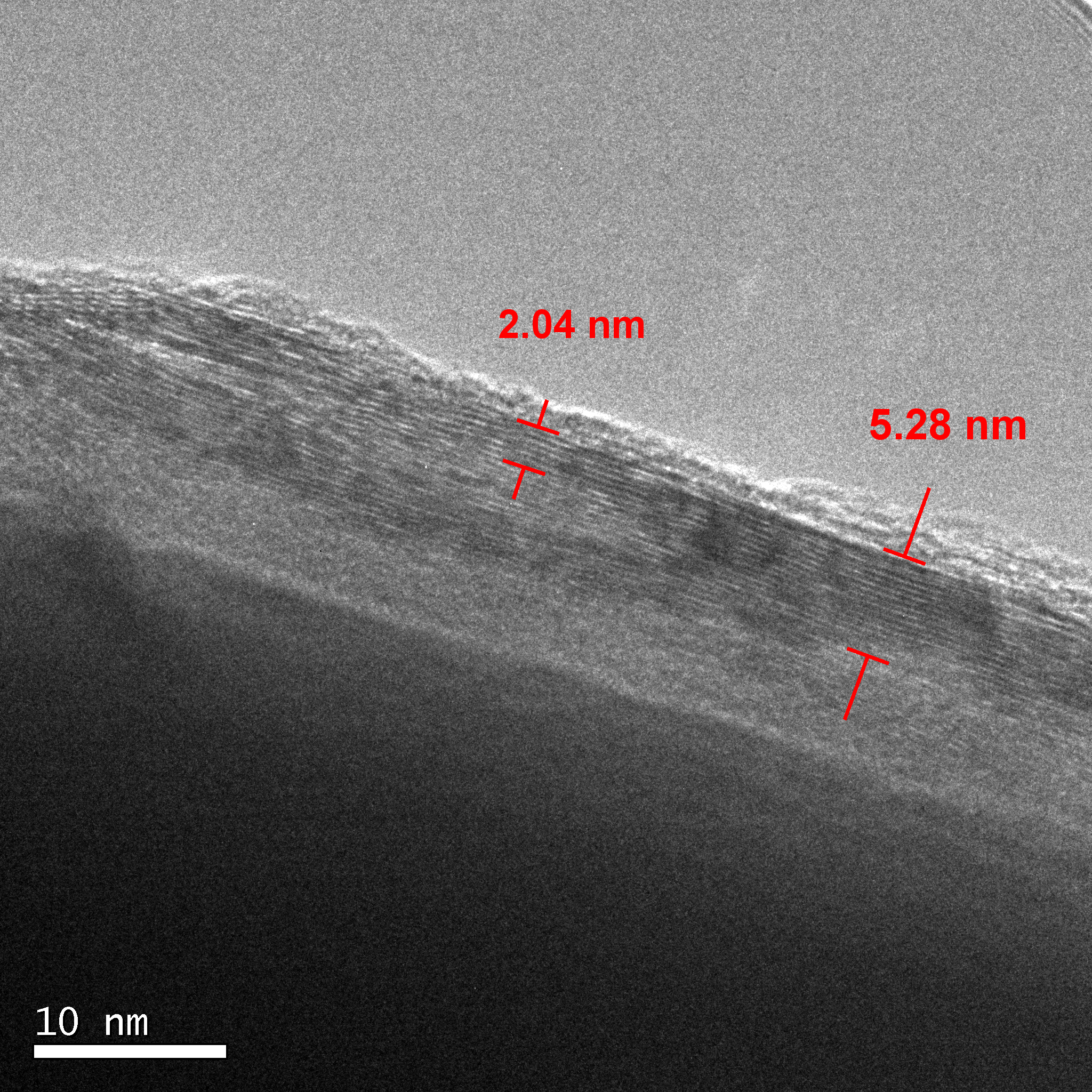 Figure 5 - TEM images of NTs deposited onto bare Cu TEM grid. Larger bundled tubes are seen with surfactant as well as smaller tubes (~2nm in diameter)
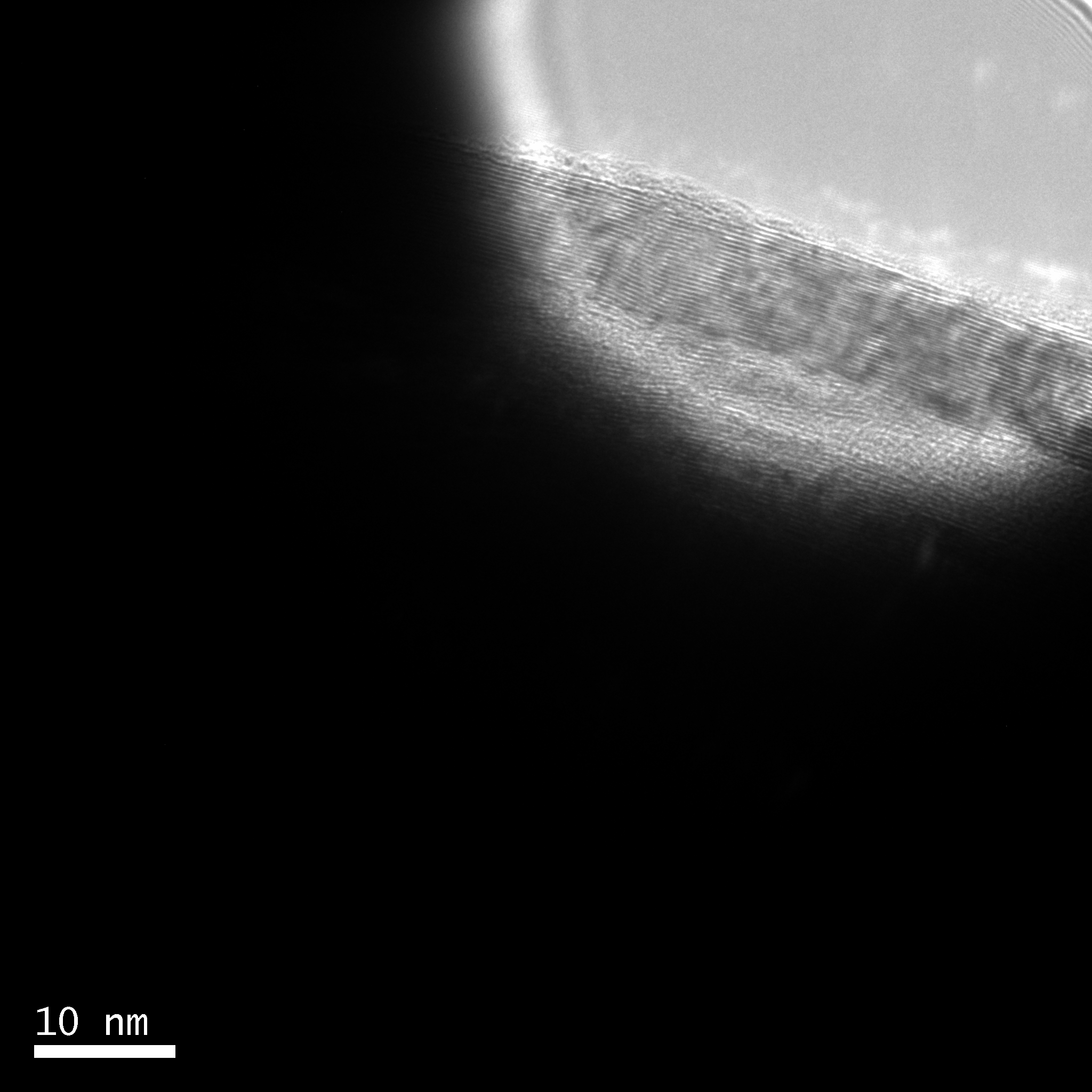
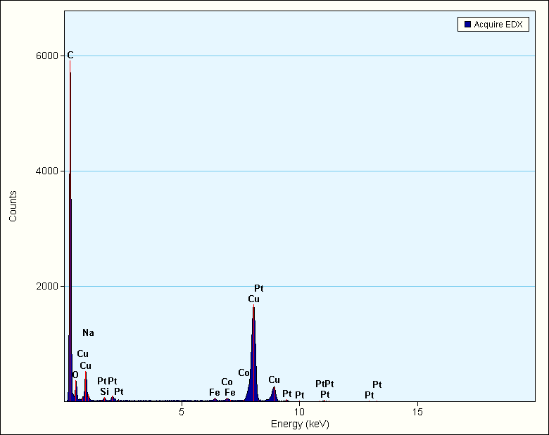 Figure 6 - (left) Focused electron beam spot on the tube for EDS measurements (right). Large signal for carbon along with surfactant and catalysts is confirmed.
Figure 4 - SEM micrographs of NTs deposited (drop-casted) onto carbon support film (TEM grid) taken at low 0.5 kV. 5. TEM & EDS
Figure 5 - TEM images of NTs deposited onto bare Cu TEM grid. Larger bundled tubes are seen with surfactant as well as smaller tubes (~2nm in diameter)
Figure 6 - (left) Focused electron beam spot on the tube for EDS measurements (right). Large signal for carbon along with surfactant and catalysts is confirmed. 6. AFM & Height Analysis
After observing the patterned ITO sample with deposited tubes on the SEM, AFM was used to accurately determine the tube diameters by measuring their heights. AFM was operated in tapping or semi-contact mode with approximate scan size of 8 um x 8 um as seen on Figure 7. Although, the regions observed by the SEM and AFM do not exactly correlate - bundle like structures were also observed similar to SEM with the AFM topographic images. In total, four (8 um x 8 um) images were taken and heights of 40 individual tubes were measured by taking linecuts approximately perpendicular to the tube long axis as seen on Figure X (right). The small background grainy structure on the order of few nanometers is likely the ITO metal coating, while the larger and taller spherical-like shapes are surfactant clumps. We note that the lateral AFM resolution is limited to around 25-30 nm which is limited by the tip radius and stage controls.
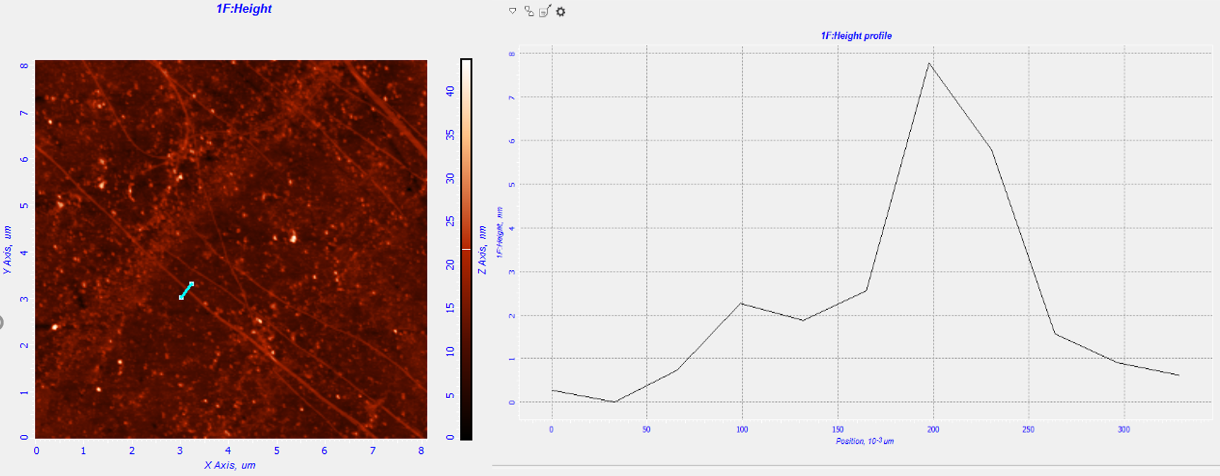 Figure 7 - (left) Topographic AFM scan in tapping mode of the ITO sample over a 8x8 um square region. (right) Height profile along blue line on left image indicates tube height of 7-8 nm.
Figure 8 below summarizes the tube diameter distributions measured by both SEM for two samples (50 tubes for the ITO sample & 45 tubes for the carbon film) and from the AFM as described above. For the SEM samples, micrographs were imported/calibrated, and tube widths were manually measured using the line tool in ImageJ. We see a clear separation in the size distribution as the AFM measures on average about 6.7 nm diameter while the SEM micrographs indicate tube diameters of about 23 and 53 nm. It is important to note that for the carbon film sample, micrographs were only taken at lower 0.5 to 0.6 kV as contamination from the beam interacting with surface and charging was readily observed - which could further make tubes appear larger. The ITO sample micrographs were taken at 5 kV which has a narrower beam spot size - potentially improving resolution to provide more accurate measurements.
Figure 7 - (left) Topographic AFM scan in tapping mode of the ITO sample over a 8x8 um square region. (right) Height profile along blue line on left image indicates tube height of 7-8 nm.
Figure 8 below summarizes the tube diameter distributions measured by both SEM for two samples (50 tubes for the ITO sample & 45 tubes for the carbon film) and from the AFM as described above. For the SEM samples, micrographs were imported/calibrated, and tube widths were manually measured using the line tool in ImageJ. We see a clear separation in the size distribution as the AFM measures on average about 6.7 nm diameter while the SEM micrographs indicate tube diameters of about 23 and 53 nm. It is important to note that for the carbon film sample, micrographs were only taken at lower 0.5 to 0.6 kV as contamination from the beam interacting with surface and charging was readily observed - which could further make tubes appear larger. The ITO sample micrographs were taken at 5 kV which has a narrower beam spot size - potentially improving resolution to provide more accurate measurements.
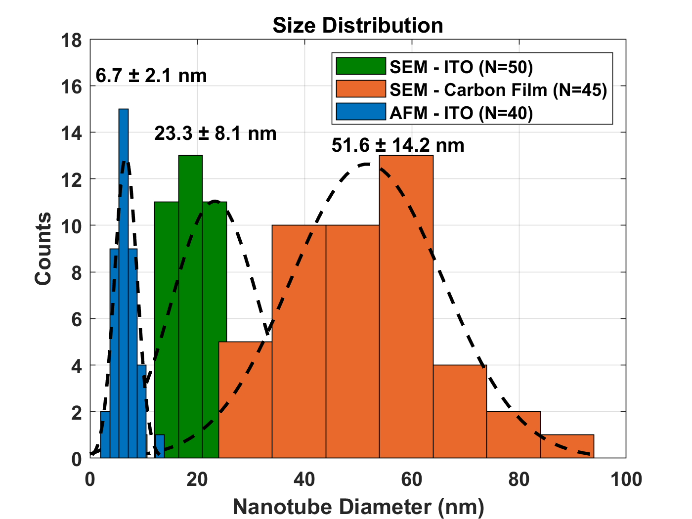 Figure 8 - NT diameter distribution across the SEM and AFM measurements. SEM measures larger apparent tube diameters possibly due to limited resolution and beam interactions with the sample.
AFM is widely accepted as the more accurate tool for measuring small nanotube diameters.
Although these measurements are not correlative (i.e. not of the same tubes), I believe the sample size is great enough to indicate that characterizing small diameter SWCNTs under SEM may significantly overestimate tube diameter compared to the gold-standard AFM. We note that typical surfactant tubes that are just spin-coated measure about 3-5 nm, so our average of 6.7 nm with AFM is in reasonable agreement considering more bundling or surfactant buildup may have occurred from drop-casting. Other groups have similarly measured larger apparent pristine tube (as grown on substrate) diameters under the SEM compared to AFM at varying operating conditions and substrate type [7]. The electron beam interacting with local electric fields from the tube may also be responsible for the diameters to appear larger [8]. Regardless, SEM can still be used as a powerful tool to characterize the overall areal density of the tubes on the patterned substrate for future correlative studies of individual SWCNTs. Near-term measurements will involve direct surface correlation from AFM of NTs using the patterned substrate with photoluminescence spectroscopy.
 Figure 7 - (left) Topographic AFM scan in tapping mode of the ITO sample over a 8x8 um square region. (right) Height profile along blue line on left image indicates tube height of 7-8 nm.
Figure 8 - NT diameter distribution across the SEM and AFM measurements. SEM measures larger apparent tube diameters possibly due to limited resolution and beam interactions with the sample.
Figure 7 - (left) Topographic AFM scan in tapping mode of the ITO sample over a 8x8 um square region. (right) Height profile along blue line on left image indicates tube height of 7-8 nm.
Figure 8 - NT diameter distribution across the SEM and AFM measurements. SEM measures larger apparent tube diameters possibly due to limited resolution and beam interactions with the sample. AFM is widely accepted as the more accurate tool for measuring small nanotube diameters.
Acknowledgments
References
1. He, X., et al. "Carbon Nanotubes as Emerging Quantum-Light Sources." Nature Materials, vol. 17, no. 8, 2018, pp. 663-670., doi:10.1038/s41563-018-0109-2.
2. Ma, Xuedan, et al. "Room-Temperature Single-Photon Generation from Solitary Dopants of Carbon Nanotubes." Nature Nanotechnology, vol. 10, no. 8, 2015, pp. 671-675., doi:10.1038/nnano.2015.136.
3. "Pure and Efficient Single-Photon Sources by Shortening and Functionalizing Air-Suspended Carbon Nanotubes." doi:10.1021/acsanm.9b02209.s001.
4. He, Xiaowei, et al. "Tunable Room-Temperature Single-Photon Emission at Telecom Wavelengths from sp3 Defects in Carbon Nanotubes." 2017 International Conference on Optical MEMS and Nanophotonics (OMN), 2017, doi:10.1109/omn.2017.8051442.
5. Lin, Ching-Wei, et al. "Creating Fluorescent Quantum Defects in Carbon Nanotubes Using Hypochlorite and Light." Nature Communications, vol. 10, no. 1, 2019, doi:10.1038/s41467-019-10917-3.
6. Hofmann, Matthias S., et al. "Ubiquity of Exciton Localization in Cryogenic Carbon Nanotubes." Nano Letters, vol. 16, no. 5, 2016, pp. 2958-2962., doi:10.1021/acs.nanolett.5b04901.
7. Li, Dongqi, et al. "Scanning Electron Microscopy Imaging of Single-Walled Carbon Nanotubes on Substrates." Nano Research, vol. 10, no. 5, 2017, pp. 1804-1818., doi:10.1007/s12274-017-1505-7.
8. Brintlinger, T., et al. "Rapid Imaging of Nanotubes on Insulating Substrates." Applied Physics Letters, vol. 81, no. 13, 2002, pp. 2454-2456., doi:10.1063/1.1509113.