University of Rochester, Materials Science Program
1. Introduction
When performing experiments on particle-based samples, it is often necessary to isolate individual particles from an aggregate setting. To maintain experiment integrity the entire measurement sequence should be based on a single sample, yet it is often nontrivial to consistently locate and isolate the same small particle (of ~ 100 nanometers) across different measurement systems.
Since the scanning electron microscope (SEM) and transmission electron microscope (TEM) are capable of imaging samples at resolutions far exceeding the diffraction limit of light, they are incredibly useful when combined with optical microscopy. The challenge then is to return to the same region of interest observed on a SEM/TEM and a light microscope. Previously, researchers identified and isolated small particles of interest by utilizing sample geographic landmarks known as fiduciary markings in both optical and electron microscopy.
An array of 4-sided asymmetrical fiduciary markings allowing both forward (top down onto the sample) and backward (through a transparent substrate) facing markings would improve common fiduciary markings to allow for sample analysis to be performed across measurement techniques and resolving power.
1. Upconverting Nanoparticle Characterization
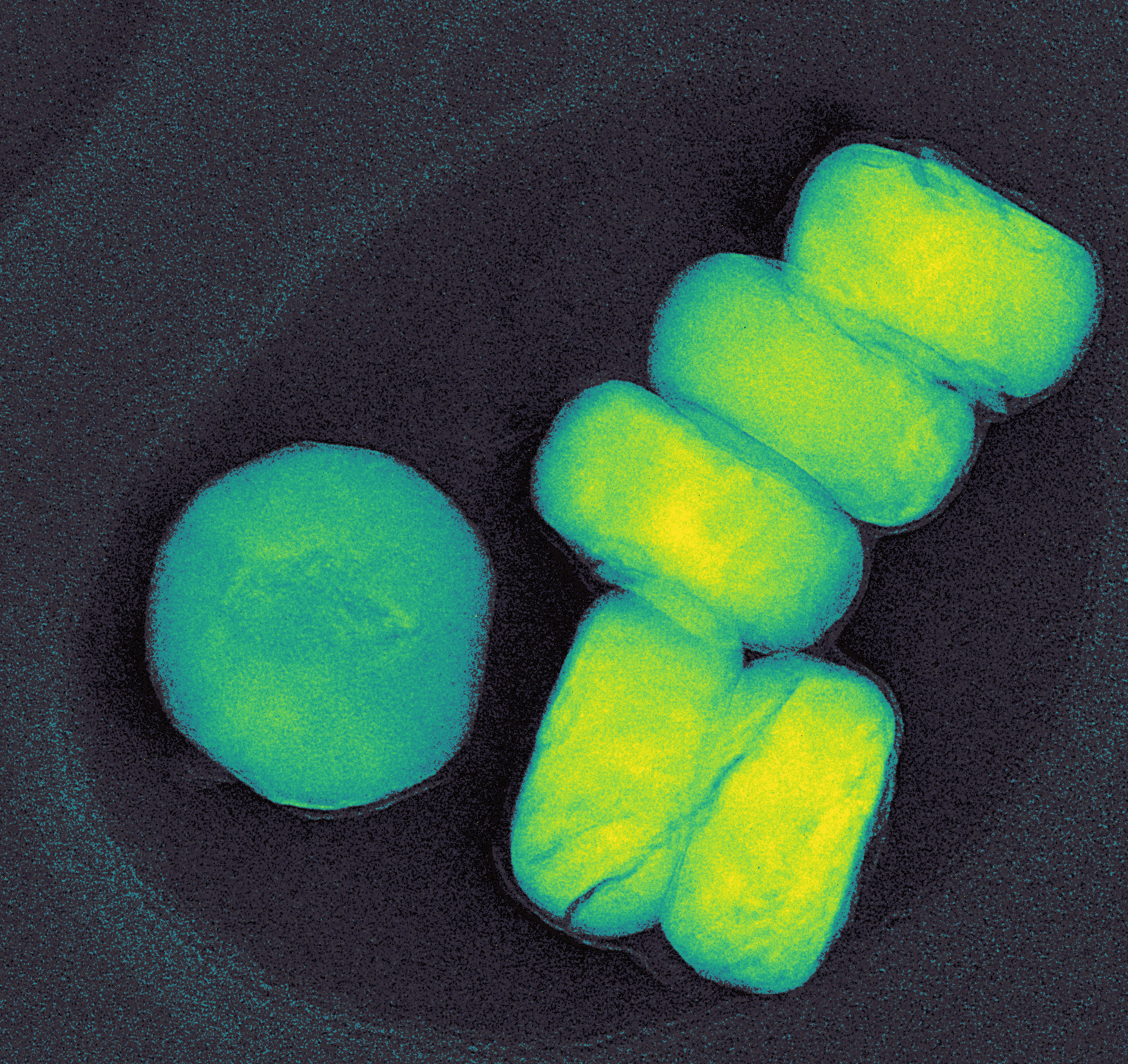
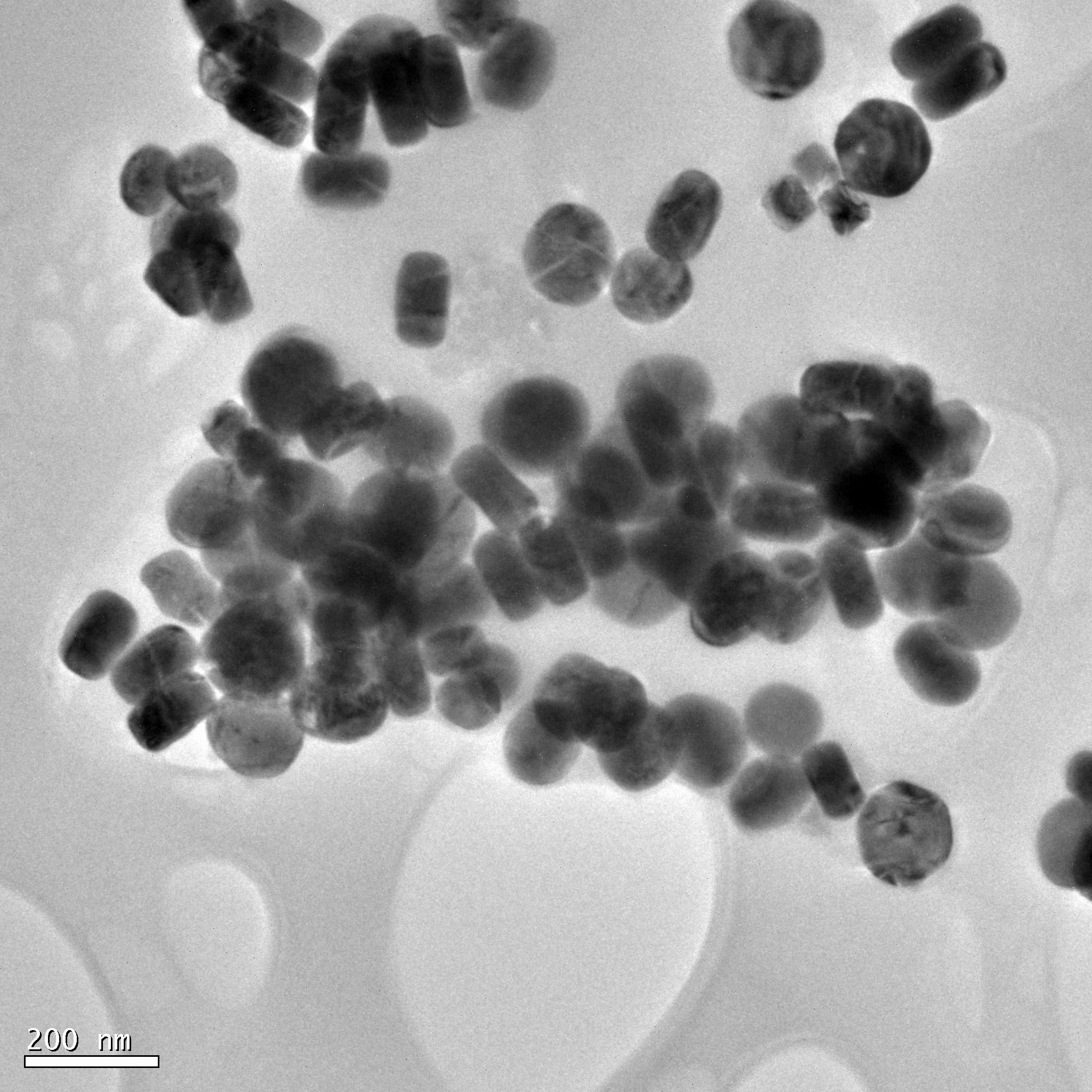
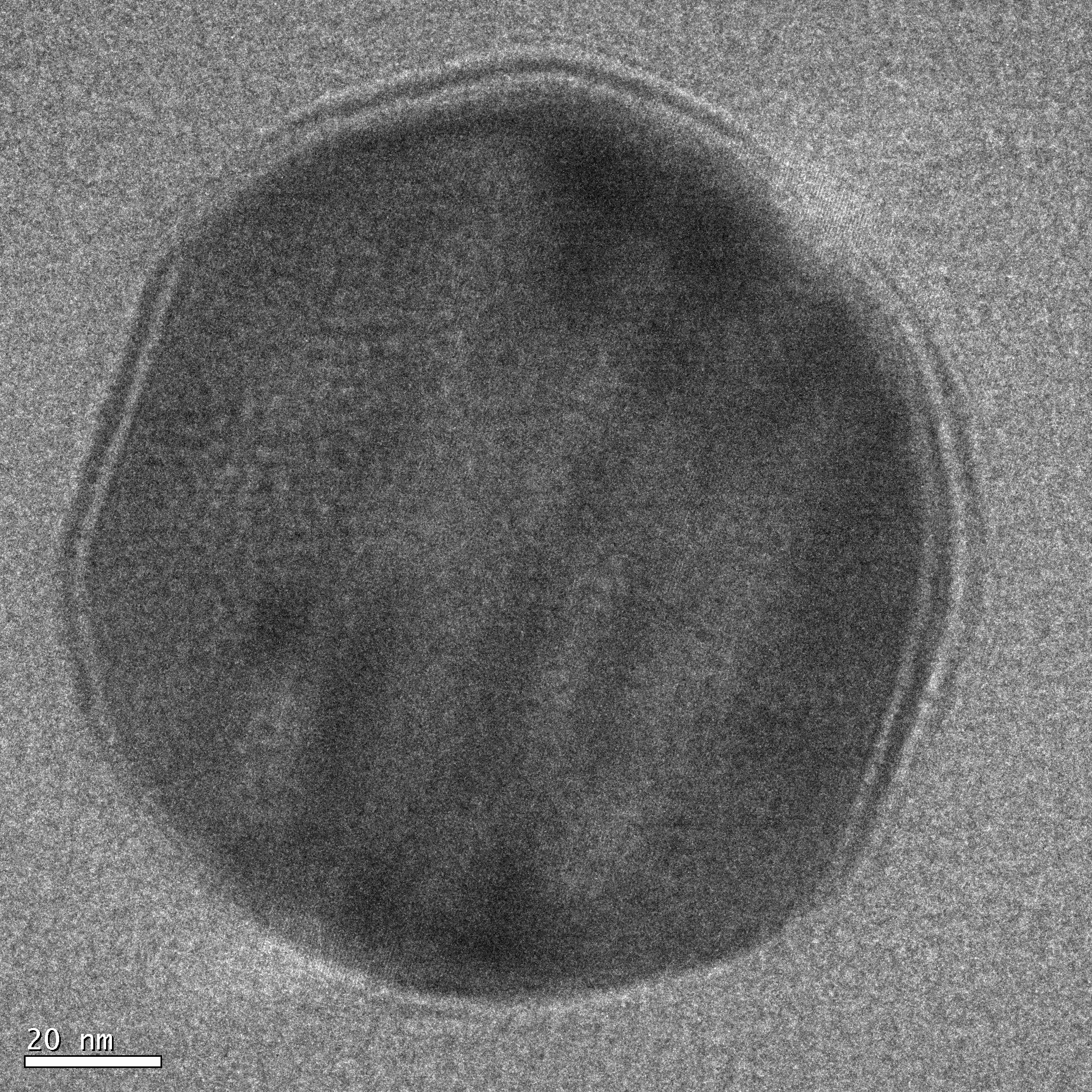
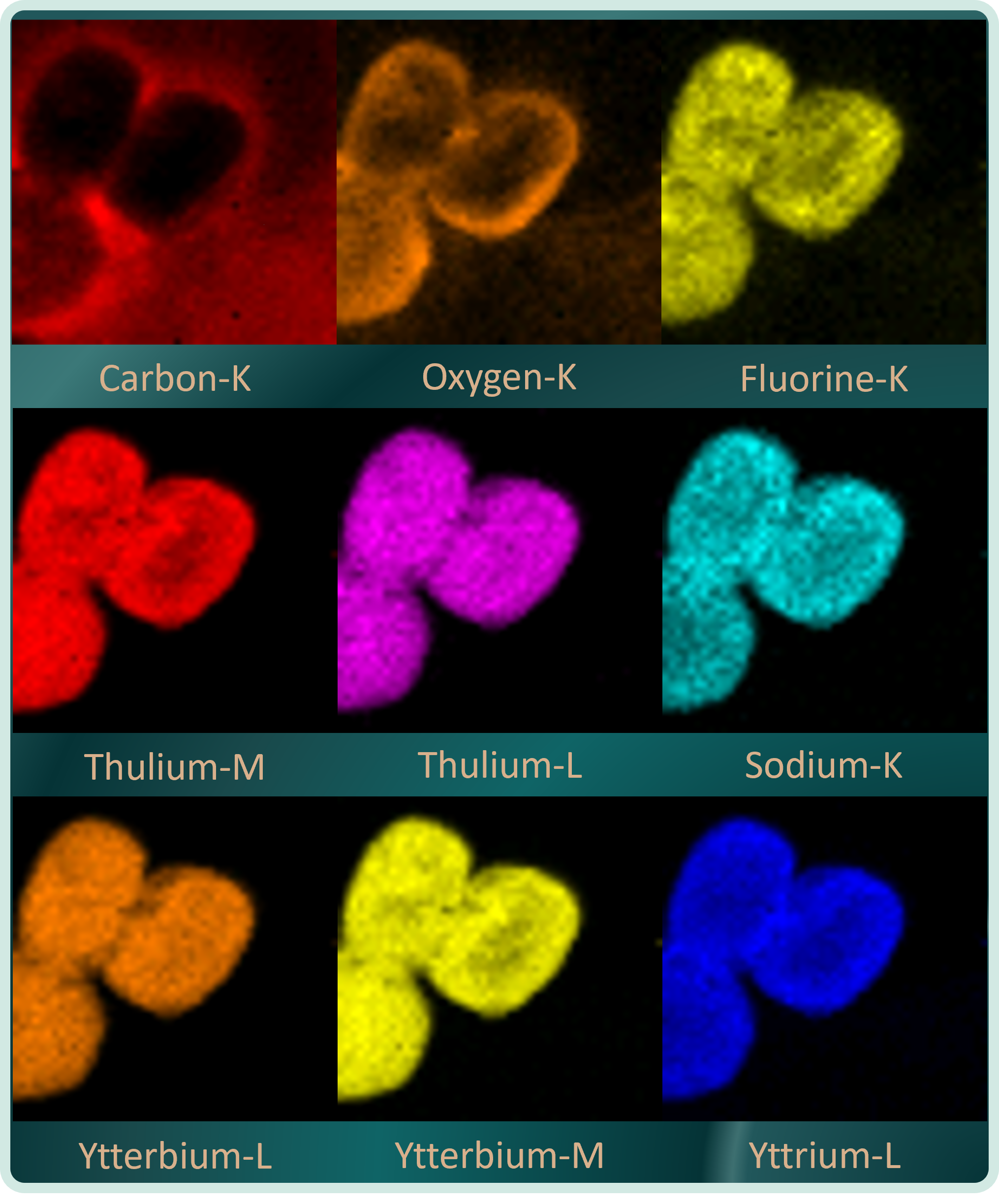
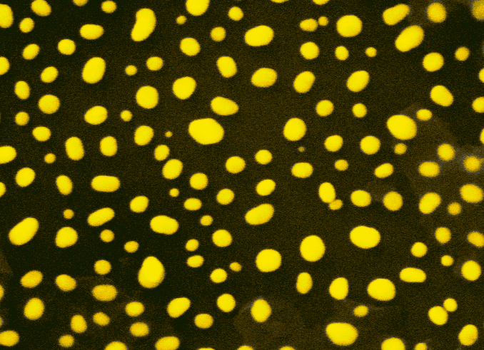
Upconverting nanoparticles (UCNPs) were dispersed along a TEM carbon support mesh. The UCNPs were purchased from a commercial supplier that claims a uniform size distribution. Since the size of the UCNPs significantly impacts the experimental results of the lab analysis it was important to verify that the manufacturer's specifications were accurate before any UCNPs were being utilized in lab experiments. The UCNPs are expected to be approximately 150 nm in diameter and consisting of a NaYF4 crystal doped with 18-20% Yb and 8-10% Tm.
The TEM images were obtained under bright field imaging conditions. The maximum image contrast was achieved by setting the image to be slightly out of focus. Several different TEM grid windows were analyzed to ensure a representative sampling of particle size was conducted.
To focus the images in the TEM the Fast Fourier Transform (FFT) was observed and the first Fresnel ring was maximized to the camera field of view. The image below needs to be adjusted for astimgatism, but represents an earnest attempt to take a high resolution image.
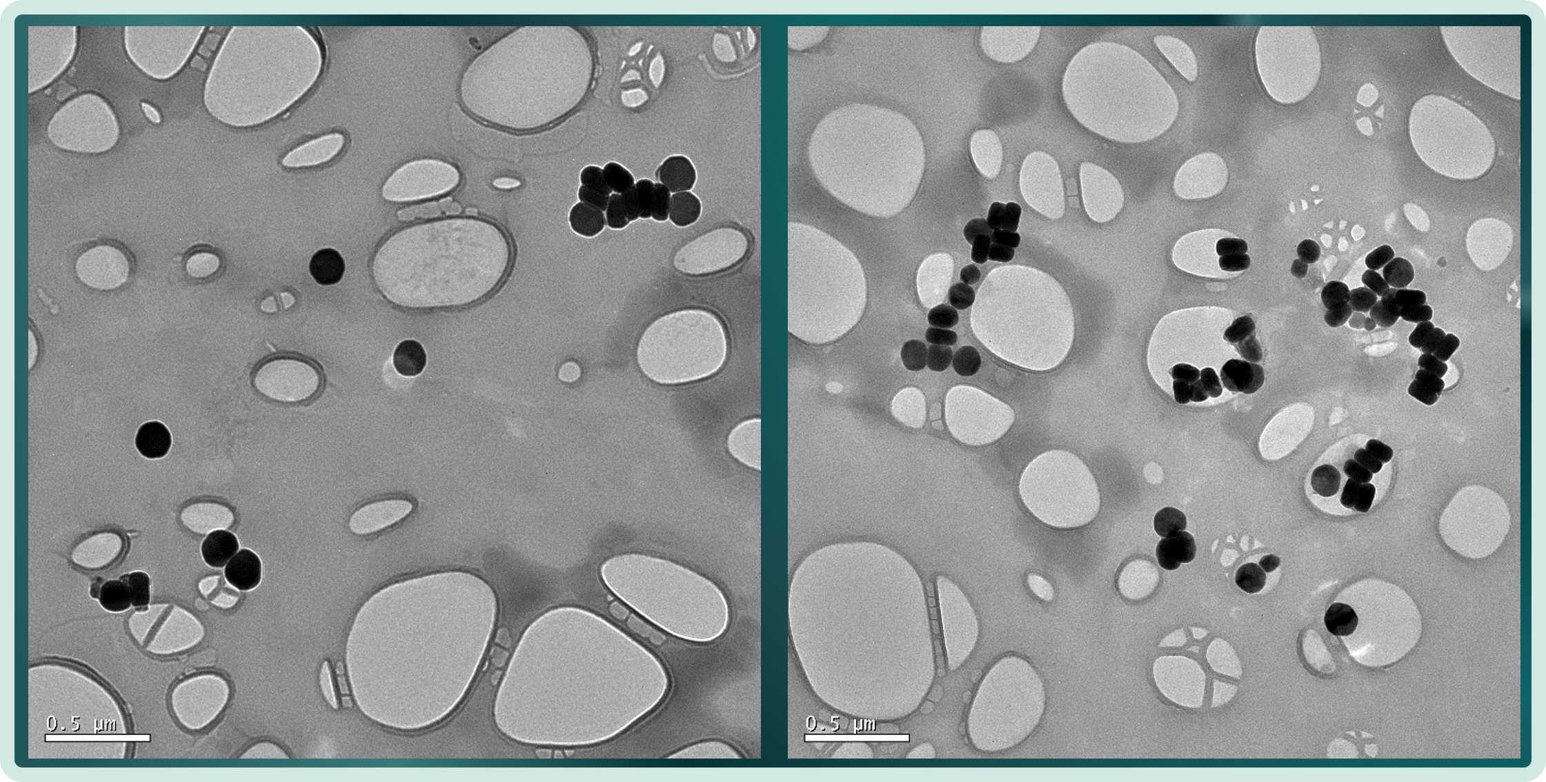
A UCNP cluster was also looked at under energy dispersive x-ray spectroscopy (EDS) to qualitatively determine the elemental species present. Manual confirmation of the elemental peaks was performed after an x-ray spectra was obtained.
2. Developing Fiduciary Markings Around Gold Nano-Islands
Several glass substrates were previously prepared by forming gold nano-islands approximately 100 nm in diameter across the surface of the substrate. Since the electrical conductivity of glass is low, a uniform layer of Pt was deposited across the surface of one sample to limit sample charging just for imaging purposes. Another sample underwent focused ion beam (FIB) patterning to form the fiduciary markings on the sample, this sample was used in subsequent research experiments.
Beam trajectories were modeled in CASINO, a Monte Carlo beam simulator. Electrons of 5kV (accelerating voltage used for imaging) and 30kV (meant to represent the Ga FIB beam) were modeled as they interacted with a 100nm gold island on top of an infinitely long SiO2 substrate. In reality, the Ga ions utilized in the FIB gun have a higher mass than electrons, which would mean the Ga ions would ablate the surface of the sample.
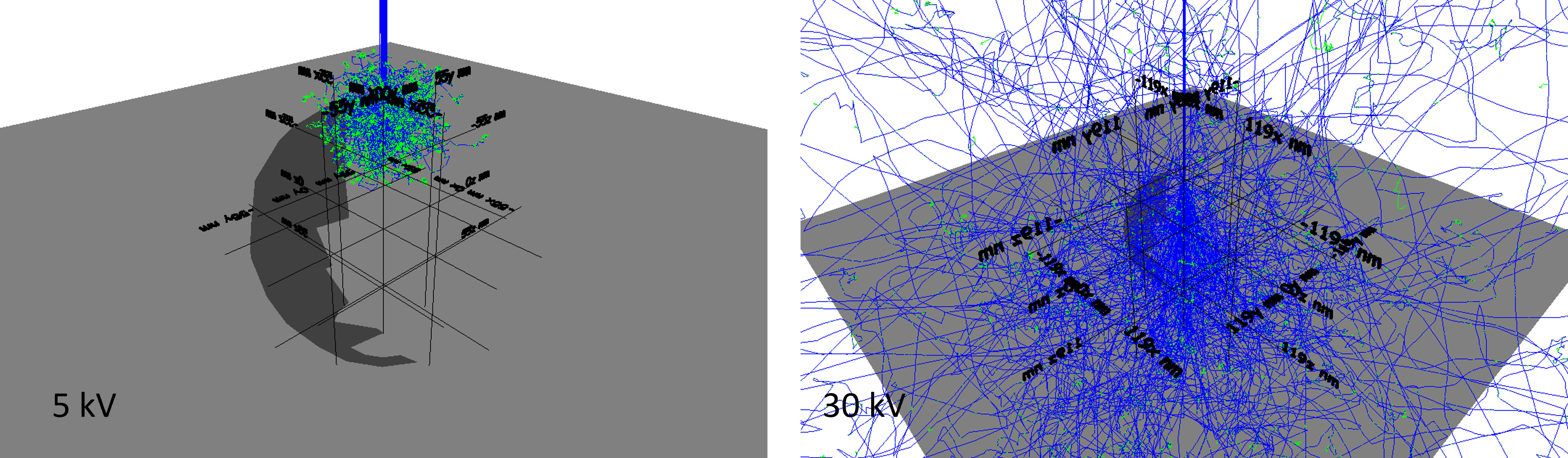
The actual sample used for the research experiments requires the use of glass (which unfortunately charges in the SEM) and that the gold nano-islands remain thermally-and electrically isolated from one another (which prevents charge from dispersing among the nano-islands). As a result, the sample with the fiduciary markings does not form the best images possible, however with proper conditions (low accelerating voltage and large aperture) an acceptable image can still be obtained.
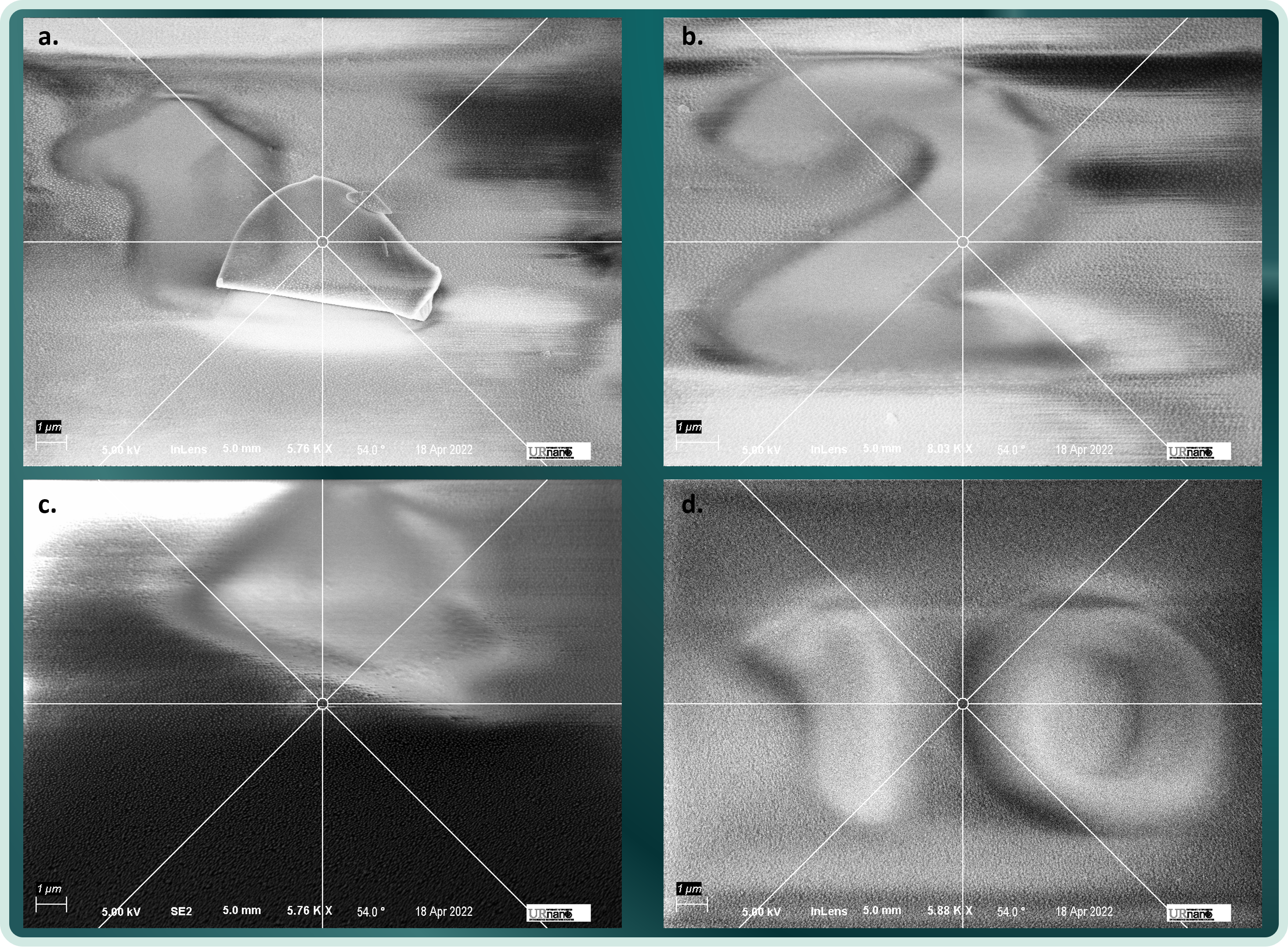
To produce the fiduciary markings, the sample was loaded into the SEM chamber and angled such that the FIB was incident on the region of interest. An image was then formed according to the pattern by bombarding the sample with Ga ions. The sample was then imaged after to confirm that the patterning was successful.
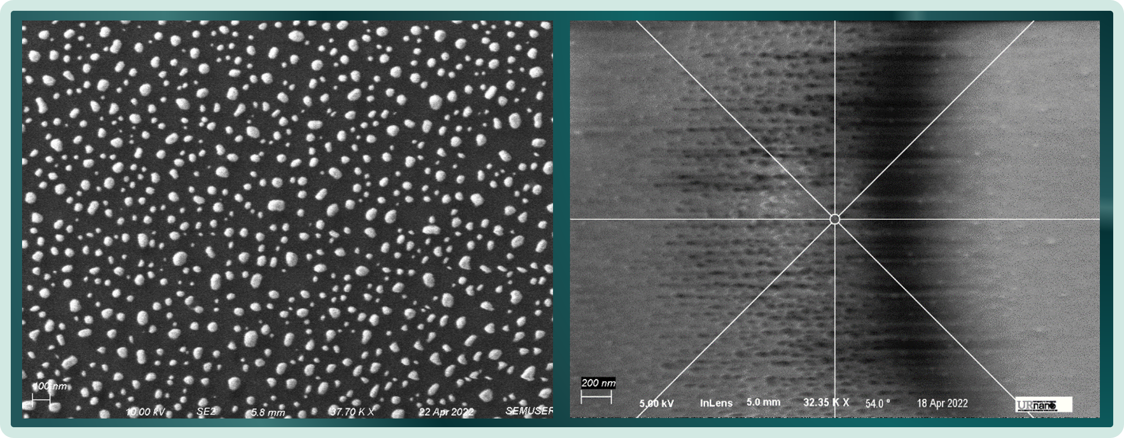
Although charging artifacts distort the images of the patterned substrate, there is a clearly defined nanoisland region that has been removed by the FIB beam. As a result of the FIB patterning, a nano-island of interest that is visible on Figure 9b can be quickly located nearby the "1" digit on both the SEM and a light microscope. Subsequent nano-islands experiments will greatly benefit from the easily locatable fiduciary markings. Both optical microscopes and the SEM should be able to locate regions of interest based on a realtive position around a fiduciary marking.
3. Conclusion
The development of asymmetrical fiduciary markings will allow for convenient identification of individual particles across different measurement techniques. As a result, experiments can be performed on a single particle, improving the reliability of research findings.
One of the more challenging aspects of this project was working through the sample charging artifacts. Sample drift and bright/dark spots were inevitable and made obtaining good images with the SEM extremely difficult. Typical steps taken to reduce charging such as using a lower electron dose produced marginally better images. If the FIB sample did not need to uphold certain thermal requirements it would be advisable for future iterations to replace the glass substrate with a more conductive transparent film, such as Indium Tin Oxide, to reduce charging.
Acknowledgments
I would like to thank Brian McIntyre for lending his expertise and assistance toward this project. I also would like to acknowledge the Nanoscale Thermal Transport Lab and Professor Andrea Pickel for providing the resources and assistance necessary to carry-out this project.
References
1. F, Adeeba, et al. "Precision of fiducial marker alignment for correlative superresolution fluorescence and transmission electron microscopy." Discover Materials, (2021).