Department of Physics and Astronomy, University of Rochester, Rochester, New York 14627
I. Introduction
Semiconductor spin qubits are a promising platform for building quantum computers, as they demonstrate long coherence time and have high fidelity. Making spin qubit devices is aligned with state-of-the-art fabrication techniques, such as photolithography and electron-beam lithography (EBL). One of the most feasible design routes for spin qubit devices is an overlapping gate architecture, which enables easy control on electrons since gates from different layers are close to each other. To fabricate such spin qubit devices, nanometer level precision is required so that all gate layers are aligned well to each other. In this project, we propose to implement auto alignment in Elionix EBL system to pattern confinement gate layers on a silicon chip.
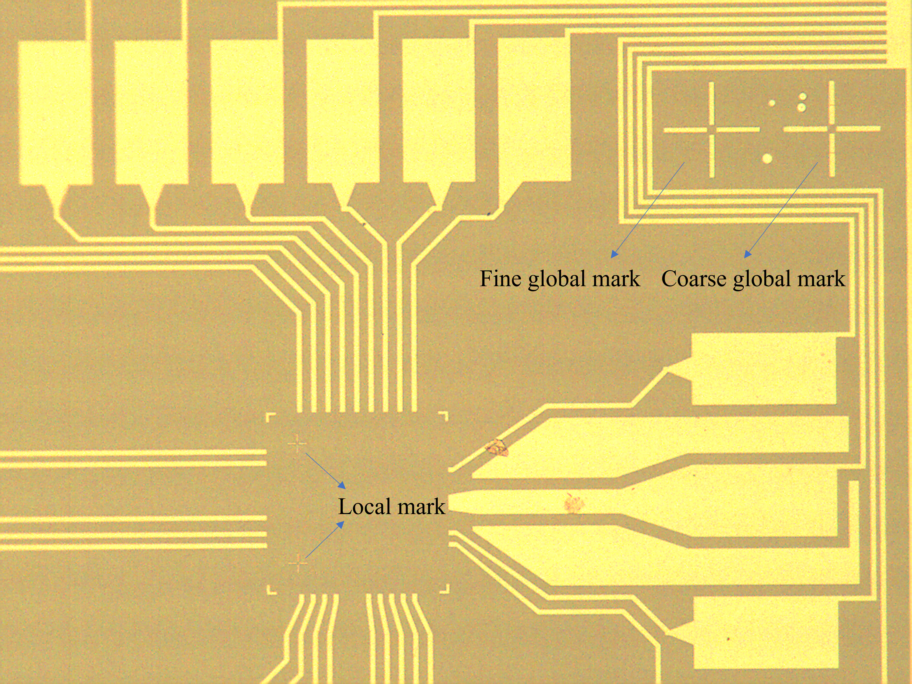
II. Device FabricationThe substrate of the device is a 6×6 mm silicon chip. Prior to patterning nanoscale gate layers via EBL, we define bond pad patterns and coarse alignment marks on the chip using the laser writer in the URnano cleanroom, where AZ5214e-IR photoresists are used for negative-tone photolithography. The silicon chip has a 2×2 array of bond pads which can host a device. After developing the chip, a thermal evaporator is employed to deposit Cr/Au with 3/80 nm in thickness on the chip. The thin layer of chromium helps gold sticking on the silicon chip, also the deposited gold makes the chip easily to be imaged in both SEM and Elionix. Figure 1 shows a light microscope image of the bond pad as well as alignment marks on the chip.
Before patterning gate confinement layers, fine alignment marks at the device level are patterned via EBL that provide a more accurate alignment between different gate layers. The current design of our spin qubit device consists of four different gate layers. For each layer, the EBL procedure includes spinning polymethyl methacrylate (PMMA) resists on the chip, making contamination dots to finely tune up the beam, aligning the pattern to previous layers, and then writing the pattern. The pattern is then developed, and aluminum of increasing thicknesses for four layers is deposited using a thermal evaporator. The chip is then lifted off, descummed, oxidized, and coated with PMMA until all four layers are completed.
A. Dose Test
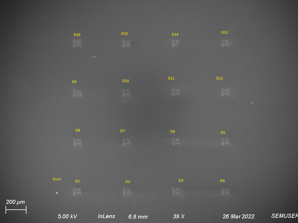
E-beam lithography functions by bombarding a focused beam of electrons in the desired areas on a sample with a coating layer of PMMA resists. Before shooting patterns on the desired sample, a dose test is done on a dummy silicon chip to determine the optimal doses for different layers that minimize the proximity effect as well as optimize subsequent EBL procedures like lifting off excess deposited metal. Our targeted patterns consist of four different layers, so we combine these four layers together in a single CAD file to do dose test more conveniently. The low magnification SEM image shown in Figure 2 presents the dose map with total 16 different doses. In the Elionix EBL system, we set the beam current as 100 pA, and sweep the current dose from 1200 to 1950 uC/cm^2, with an increment of 50 uC/cm^2. The dose test involves writing each of the layer at a series of different dosages. After exposure to electron beams, we develop the chip in MIBK:IPA solution, deposit aluminum, and lift off excess metal. Then, the patterns with different doses are ready to be imaged in the SEM to see which dosage is optimal for each gate layer.
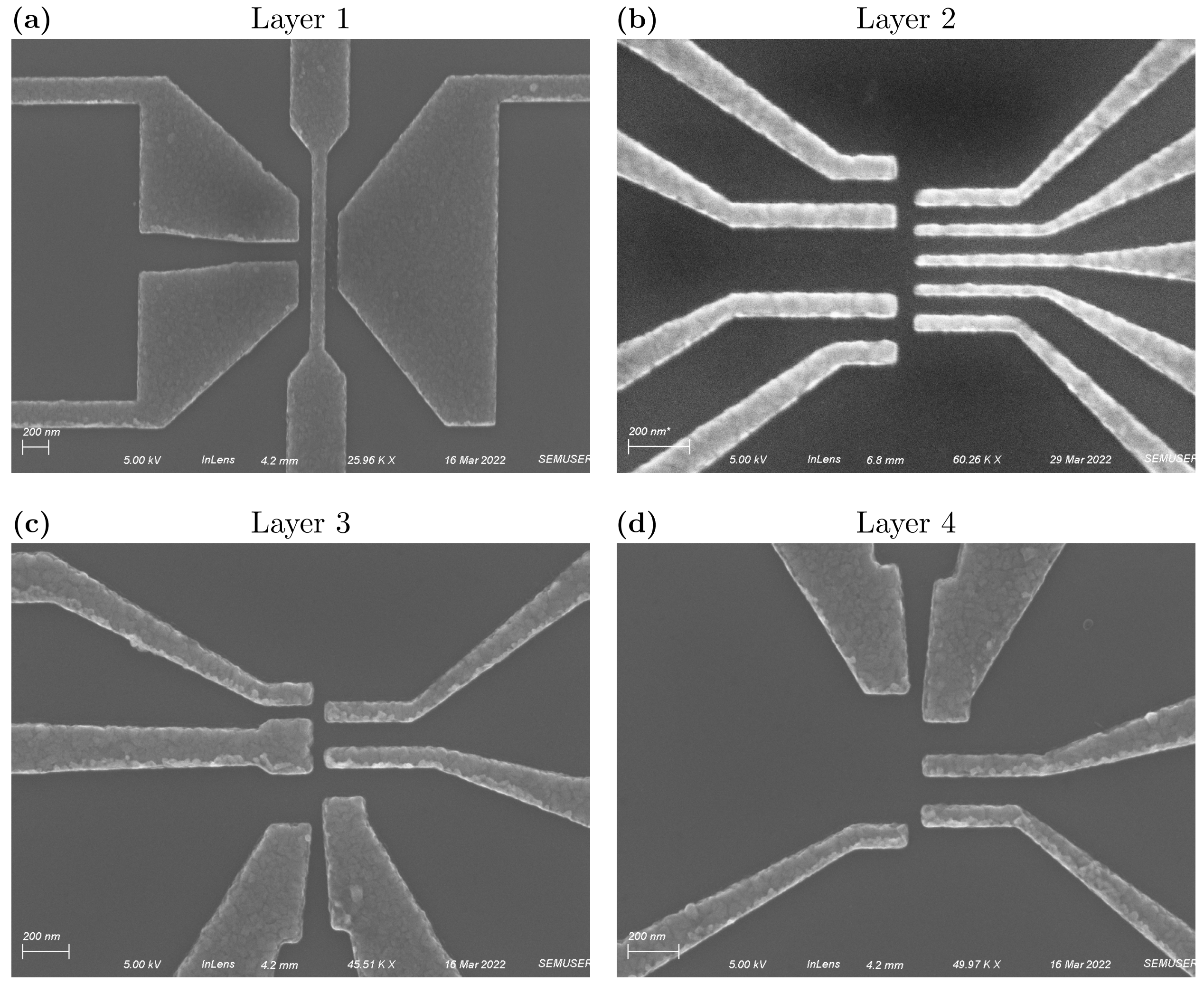
After comparing a bunch of SEM images for different layers with various doses, we determine that the optimal dose for our patterns is 1500 uC/cm^2. Figure 3 shows the SEM images for all four layers written by the 100 pA beam at a 1500 uC/cm^2 dosage. All patterns show up clearly and nicely, with neither over-exposure nor under-exposure. Since we deposit a thin layer of aluminum with just 30 nm thickness on the silicon chip, we choose a low accelerating voltage as 5kV as well as the InLens detector compatible with a short working distance 4.2 mm to image the gate layers. In this case, most interaction volume will lie within aluminum rather than silicon, so that more signals from aluminum gate layers will be collected, which is better for us to tell which dose is optimal for different patterns.
B. Alignment MarkTo implement auto-alignment in Elionix to align all four gate layers together, a set of alignment marks are used during writing. The alignment marks are cross marks deposited by gold as shown in Figure 1. When Elionix searches the mark during writing each layer, some resists on the mark arms are exposed. Thus, some aluminum will be deposited on mark arms as shown in the secondary electron SEM image in Fig. 4(a). In order for Elionix to search the marks accurately, we increase the search scan position for different layers. Figure 4(a) clearly shows that there are four lines on each arm of the marks, which confirms the search scan position settings in Elionix.
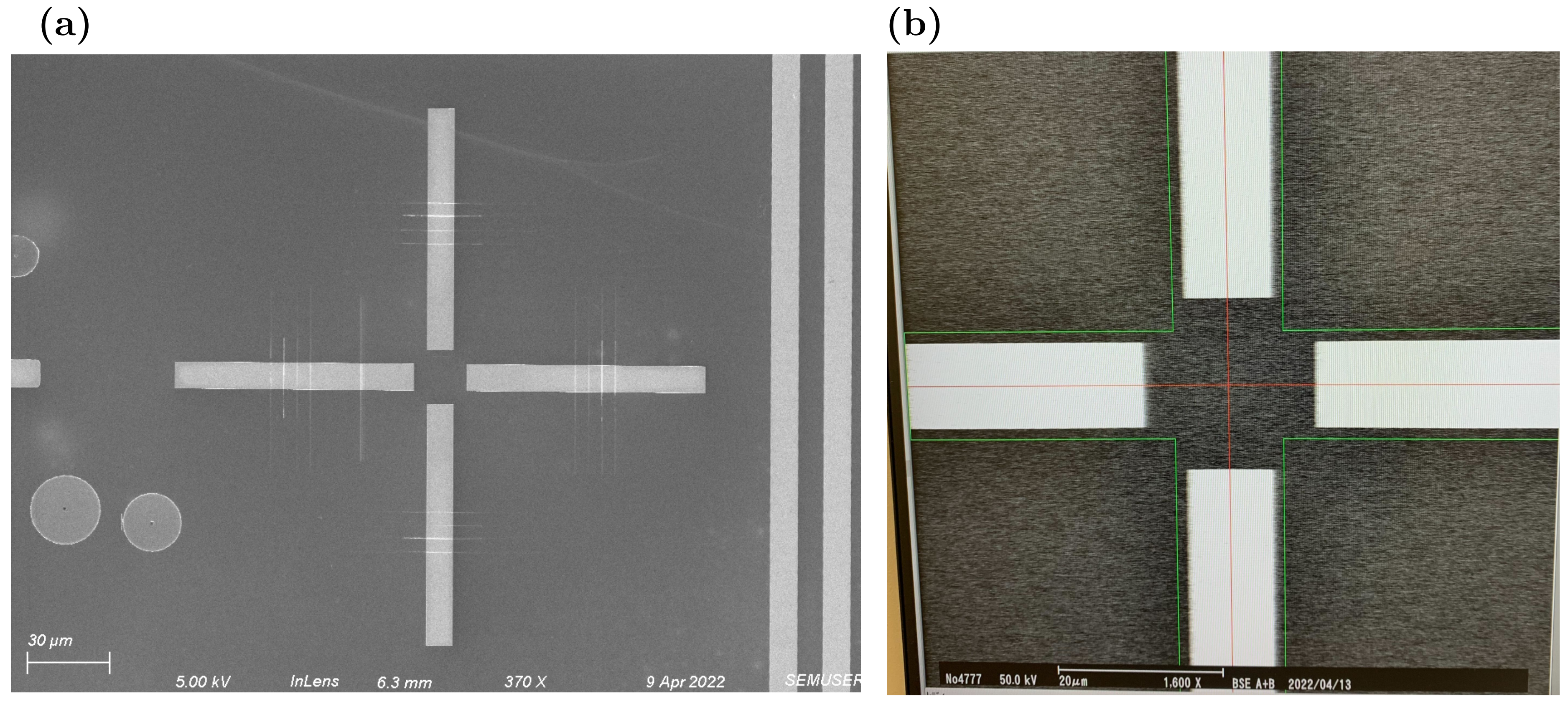
Elionix is an EBL system, but it also has an SEM with both secondary electron and backscattered electron detectors. Gold is an element with a high atomic number, so that gold will produce more backscattered electrons than silicon or aluminum. In order to get more signals from gold marks rather than silicon chip or aluminum gates, the backscattered electron detector is used in Elionix to search for the gold marks, which is shown in Fig. 4(b). The area with gold is much brighter than the area without gold, since gold can produce more backscattered electrons than other elements on the chip. This sharp contrast and brightness of the backscattered electron image is vital to search the gold marks accurately in Elionix, which is helpful for aligning different layers well.
C. Auto Alignment ResultsTo implement auto alignment in Elionix, we first change the control type as "AUTO" for both global marks and local marks in search settings. Subsequently, several parameters in the search settings such as scan feed pitch, the tolerance of the algorithm, and cross mark search position are changed to optimize the mark search algorithm.
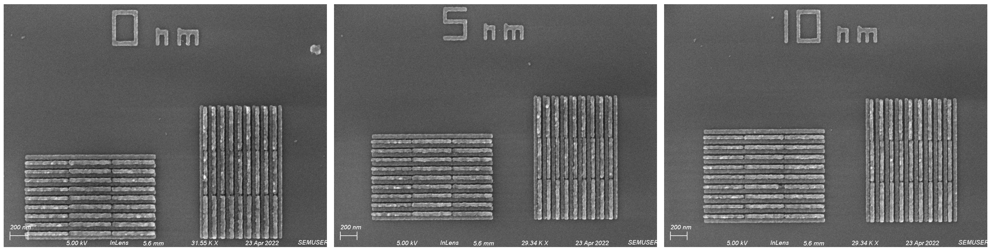
In order to get a first glance of how alignment works for each gate layer, we write dummy grating patterns along with gate layer patterns near the device region, as shown in Figure 5. The gratings on the left/right show how alignment works in the x/y direction. The long metal grating is deposited together with the 1st layer, and three short metal gratings are deposited with subsequent 2nd, 3rd, and 4th layers. When the short grating touches the long grating, it indicates that there is misalignment between the 1st gate layer and subsequent three layers. As seen in Figure 5, the misalignment is around 5-10 nm in either x or y direction. This tiny misalignment is within the design tolerance of 10 nm, so that the auto alignment process realized here is promising for making silicon spin qubit devices.
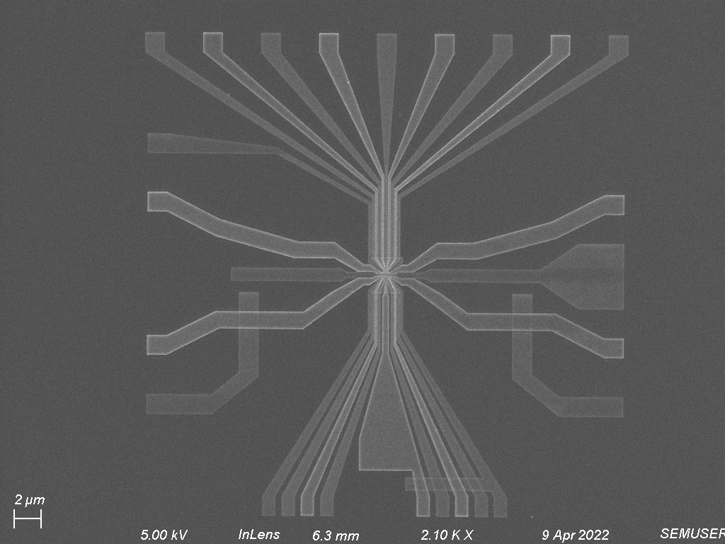
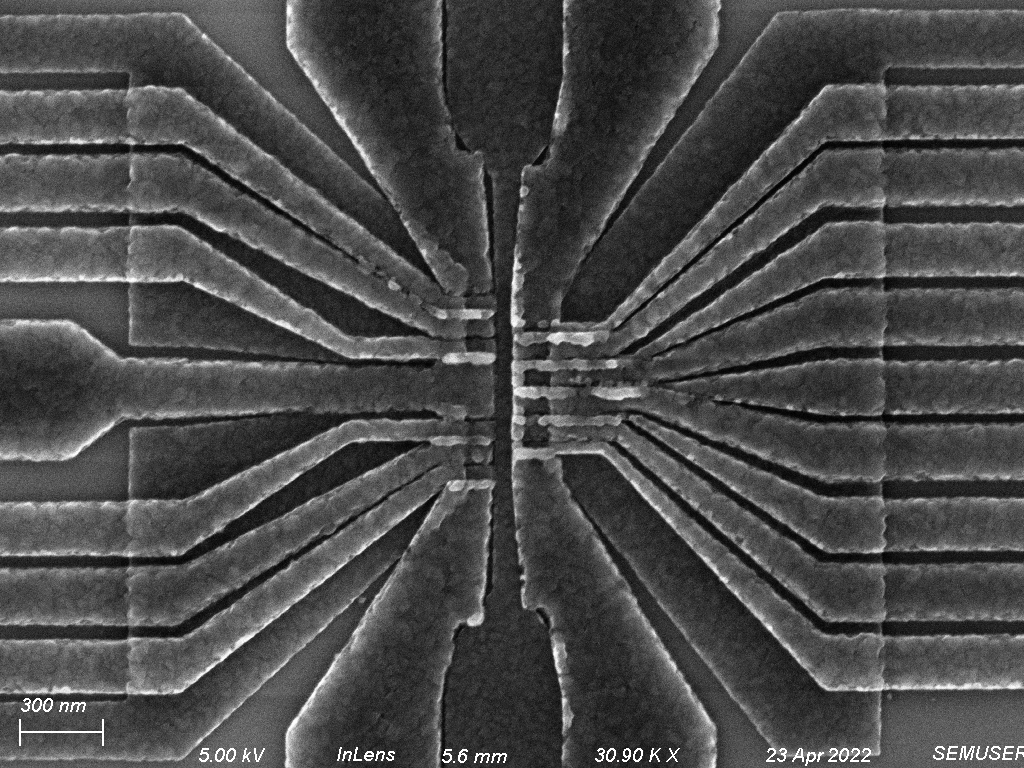
The real test of alignment comes from how well the fine inner features of the device are patterned together. Vividly, the alignment for different layers is not only to stack together four layers of the device shown in Figure 3, but also to align them together within the design tolerance both in x and y directions. The left side image in Figure 6 presents the four-layer nanostructure device on the big picture. Elionix is an intricate EBL tool, so that the device looks crispy under the microscope. Zooming in to the central region of the device gives a high magnification SEM image of the device, as shown in Figure 6 on the right. Here, the alignment between four layers is very nice. The alignment along the y axis is very good, so that all gates run parallel down as shown in the image. However, there is slight misalignment in x direction, as the left features have a slightly larger overlap with the central bridge than that of the right features. Based on the grating images shown in Fig. 5, we estimate that the misalignment here is around 5 nm, which is within the design tolerance as 10 nm.
III. Conclusion and OutlookIn conclusion, by aligning gate layers to a set of global marks and local marks on the chip, we develop automatic electron beam lithography procedures in Elionix for the fabrication of multilayer nanostructure devices. The alignment tolerance is achieved within 10 nm so that different gate layers are well aligned with each other, which is suitable for the silicon spin qubit design. However, a substantial number of alignment tests are still necessary for obtaining statistical and reliable information about how auto alignment works in Elionix for the settings we have chosen so far. We plan to push it forward in the future project.
AcknowledgmentsI would like to sincerely thank my instructor Brian McIntyre for insightful suggestions on taking SEM images. I am also grateful to Elliot Connors, Yadav Kandel, and John Nichol for enormous assistance and encouragement on this project.