University of Rochester, Department of Physics
1. Introduction
Quantum Computation is starkedly different than its classical counterpart. Classical computation is built on the foundation of classical bits that are either on (1) or off (0). Quantum Computation, on the other hand, uses quantum bits - more commonly referred to as qubits. These qubits have the ability to be in a superposition, a mixture if you will, of states i.e., a qubit can be both on (1) and off (0) at once. This allows for quantum computation to carry out multiple simultaneous calculations and work faster. In principle, any quantum object that has two states (polarization of light: longitudinal or transverse, spin of electron: up or down, etc) can be used as a qubit. Among them, spin qubits show a promising way forward.
Spin qubits have long coherence time. Electron spins maintain coherent phase for extended period of time which is vital for computation. Spin states naturally communicate via Heisenberg exchange coupling. However, these interactions are short ranged. This necessitates the coupling of spin qubits to something that can communicate in a longer time and space scale. One of the best candidates for such purpose is the spiral resonator. To attain the necessary coupling strength, the resonators need to be extremely small (pitch of roughly 250 nm - 1 um(micrometer)). While constructing structures of this scale is doable using electron beam lithography (EBL), owing to the geometry of spirals, there are numerous finely spaced structures. In this realm, proximity correction becomes paramount.
To use EBL for pattern creation, one starts with an electron resist on a substrate. For this project, Polymethyl methacrylate(PMMA) on silicon was used. A thin layer of PMMA was coated on a clean silicon chip. While mostly used as a positive tone resist, once the dose of electrons exceeds a threshold, PMMA also acts as a negative tone resist. During EBL, the electron beam with a specific current rests on a part of the sample for a preconfigured period of time - called dwell time. The combination of dwell time and beam current results in the deposition of a specific dose of electrons on the resist. Once PMMA receives the necessary dose of electrons, the long chain structure of the molecule breaks down into smaller, chain scissioned, structures. The exposed chip can then be developed in an appropriate developer. A 3:1 mixture of IPA (Isopropyl alcohol) to MIBK(Methyl isobutyl ketone) dissolves the short chain structures while keeping the long chain structures of unexposed PMMA as is. While making such small structures separated by fine spacing, constant dwell time across the sample will not work as some parts of the sample receive more electrons than intended because of the forward scattering of electrons in PMMA as well as the backscattering of electrons from the substrate. These scattering effects are collectively referred to as proximity effects and need to be corrected by simulating the spread of electrons and modifying the dwell time accordingly.
Before development of the exposed chip, the clamp accidentally scratched the device surface which mechanically developed the scratched region of the chip.
I. Dose TestingBackscattered electrons have a more prominent proximity effect than forward scattered electrons. This can be seen by a simulation of the interaction volume of the process as follows:
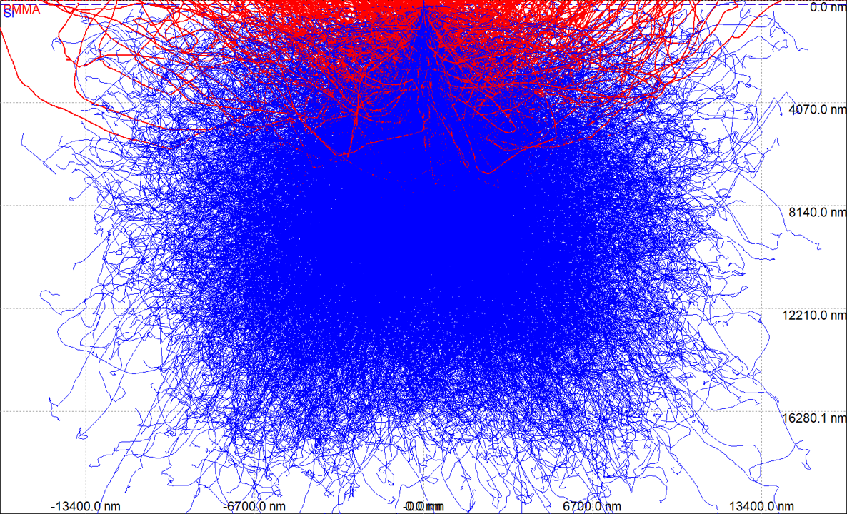
After the simulation, the spread of electrons is approximated by a point spread function. The parameters of the function are noted and used to modify the dosage time for different regions of the spiral.
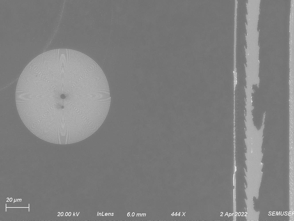
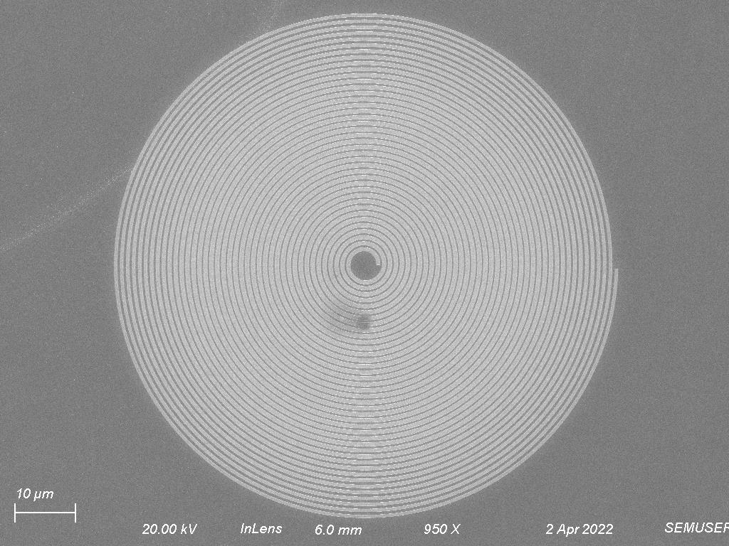
This was done primarily by using a proximity effect correction (PEC) algorithm developed by the Nichol Group called urpec available on GitHub. Following PEC, an array of spirals are drawn on a single chip where the electron dose varies in a controlled fashion - usually a range of electron dose is swept through to find the optimum dose for the spirals which is determined by SEM inspection.
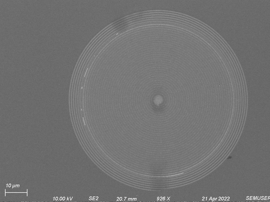
II. LiftoffFollowing development, the exposed regions have trenches in the shape of spirals. Any choice of metal can then be deposited on the chip surface. The metals fill in the trenches and also accumulate on top of the PMMA present in the unexposed region. Then, the chip is dunked in hot acetone for 'lift off' - which removes the PMMA from the unexposed region along with the metal on top of it thus only the metal spiral is left on the chip. Special caution needs to be taken during lift off to ensure all the unexposed PMMA gets removed. If not, a higher layer of metal remains between the spiral layers as follows:
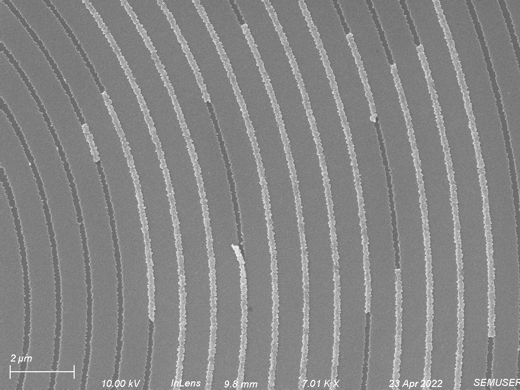
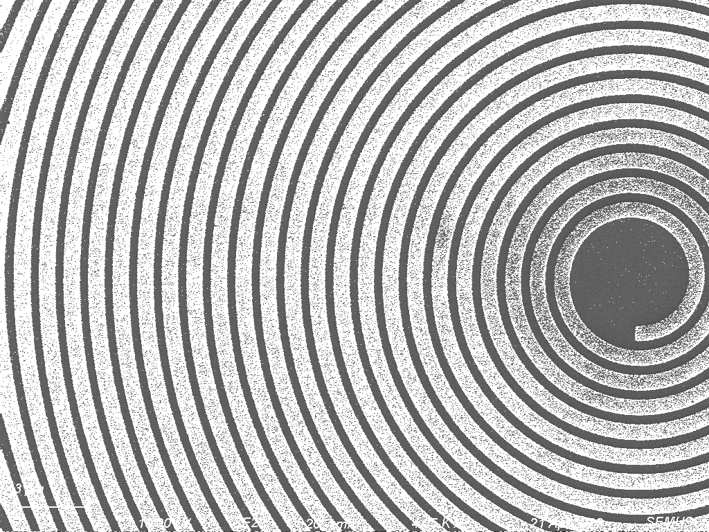
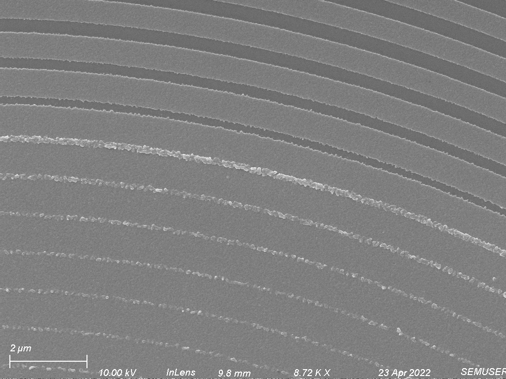
Observe a spiral with a 'good' electron dose:
While the spiral shape can be easily distinguished, with separation between the spirals also visible, upon further inspection, this spiral was also overexposed:
The spirals were designed with the same width as the spacing between the spirals. We note that this is not the case for the spiral observed. This is a consequence of overexposure. As the regions between the spirals got overexposed, upon development, a spiral trench wider than intended formed and resulted in a narrower spacing with thicker spirals. Since this was the lowest dose we started with for exposure, the rest of the spirals got overexposed as well and in increasing order.
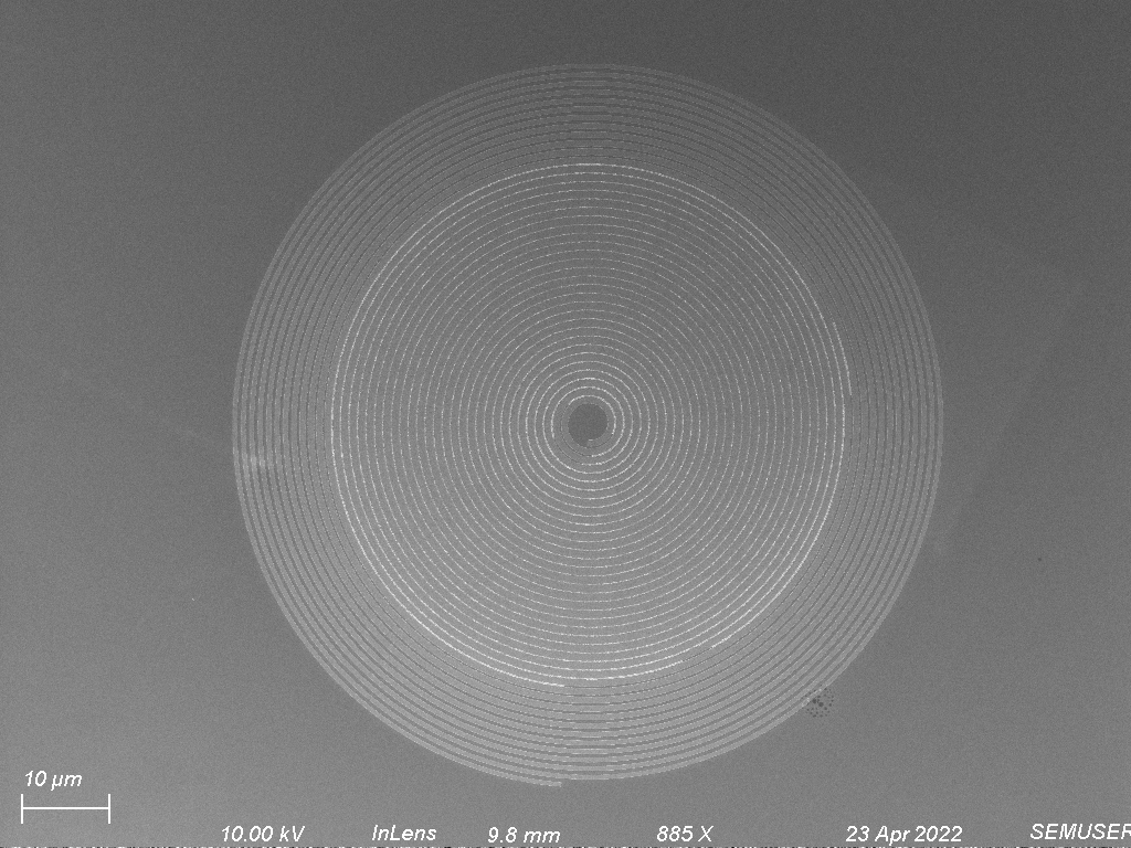
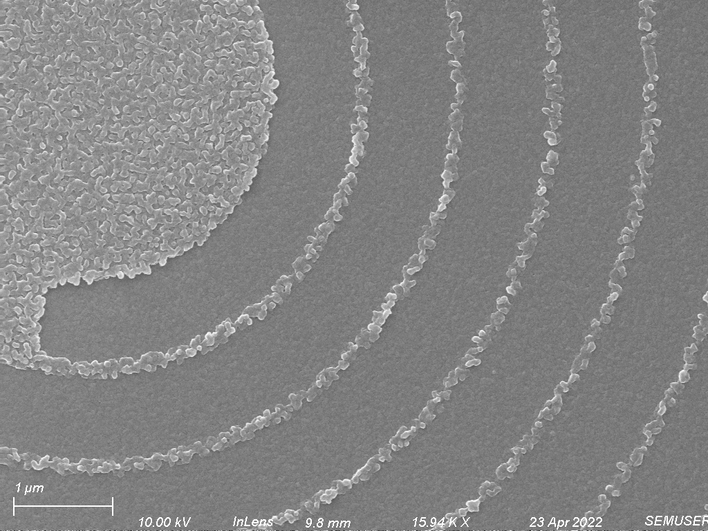
When the regions between the spirals get overexposed, within the postive resist PMMA threshold, the entire region undergoes chain scission, and upon developing, instead of a spiral trench, a wider circular trench is formed and thus metal deposition leads to a metal disc as opposed to a spiral as seen in the figure below:
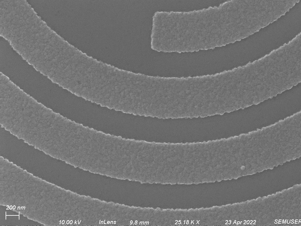
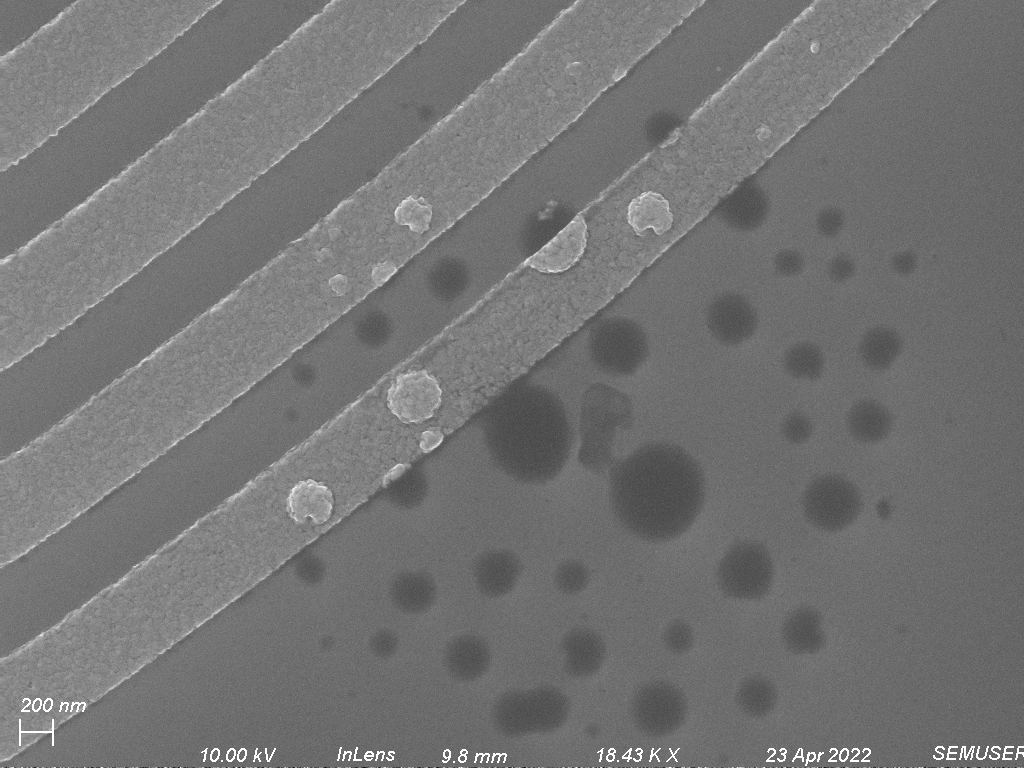
As the electron dose kept increasing for later spirals, an interesting phenomenon was discovered: variation in the height of metal layers:
Observe that the thickness of the layer decreases as we go towards the center of the spiral. This layer of metal continued all the way to the inside of the spiral, with the entire inner region filled with this layer of metal.
To answer the age old question: hole or bump, the sample was tiled and imaged:
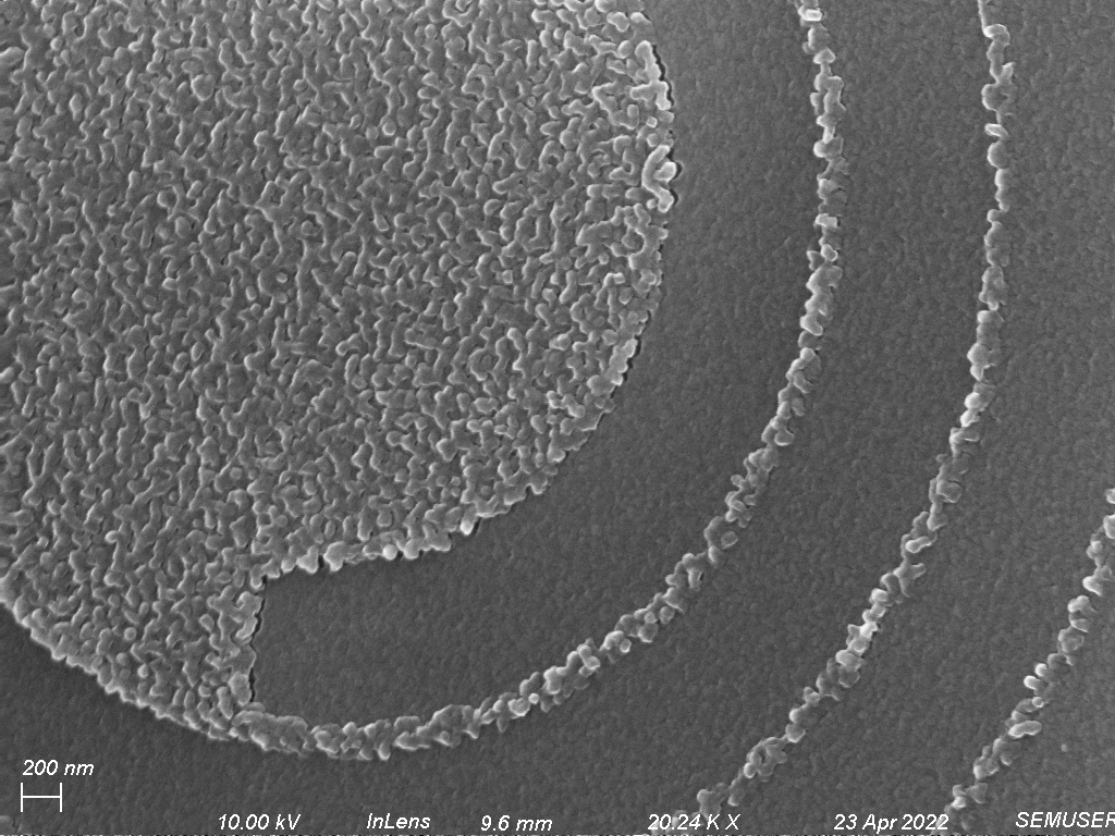
The different layer of metal was thus determined to be at a higher level than the spiral metal. This analysis was also supported by Atomic Force Microscopy (AFM) imaging and the height profile generated for the region:
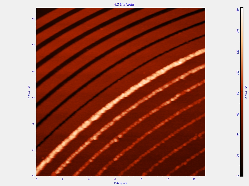
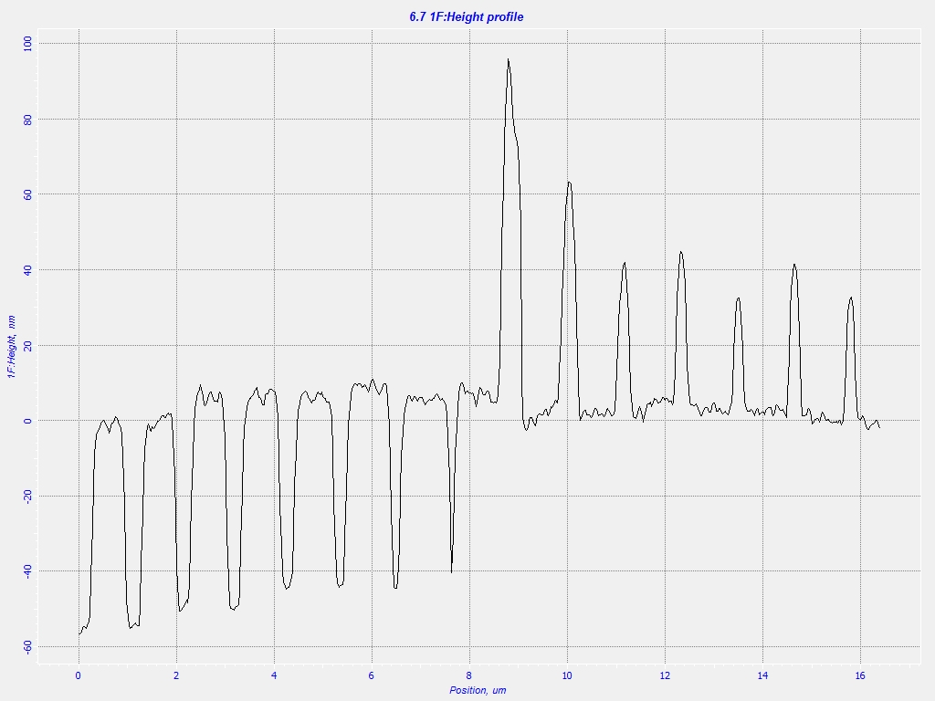
Observe that the mystery spiral of metal is highest when it first forms, decreases as we go towards the center of the spiral and evens out in height as we get to the center of the spiral. A running theory for these taller layers is the negative tone resist behavior of PMMA at higher electron dose. When the electron dose exceeds a certain threshold, PMMA polymerizes, and starts behaving as a negative resist. Polymerized PMMA does not get dissolved during development and thus in the regions exceeding the threshold, a layer of PMMA remains. As metal is deposited uniformly across the chip, the regions containing the layer of PMMA end up with an additional height than the neighboring regions, and thus the metal there is taller.
While the explanation of the negative tone resist of behavior of PMMA seems to initially make sense, it does not completely explain the thickness of the taller metal layer decreasing as we go towards the center of the spiral. If indeed the taller layer is because of over electron dose, we would expect the thickness to increase since we expect a higher interaction volume overlap as we go towards the center and thus bigger regions of polymerized PMMA. Additionally, PMMA acts as negative tone resist only in extremely high electron dose, roughly 100 times the dose required for positive tone resist[2], and at no point during the exposure did the electron dose reach such high levels. Why the metal layer is the tallest and gets shorter and narrower as we go inwards is ... .
Also of some interest was the following image:
Making nanoscale patterns using EBL runs into a heap of complications most prominent of which is proximity effects. As discussed in this report, over exposure of PMMA results in many different deviations from the intended pattern, some understood and some not. As proximity effect is one of the major contributors to over exposure, it needs to be a prime consideration while making such structures. Algorithm such as urpec is a valiant attempt at mitigating proximity effects, but it can not completely correct them. Rather than trying to completely correct them, getting them corrected just enough to obtain a good enough sample is usually advisable.
Acknowledgments
I would like to sincerely thank the great microscopist: Brian McIntyre for his support on this project, Yadav Prasad Kandel for his guidance and encouragement, and Dr. John Nichol and the Nichol Group for all of the resources and assistance.
References
1. Y. P. Kandel, H. Qiao, and J. M. Nichol, Perspective on exchange-coupled quantum- dot spin chains, Appl. Phys. Lett. 119, 030501 (2021)
2. A C F Hoole et al 1997 Semicond. Sci. Technol. 12 1166