Device Design and Fabrication
Since thermoelectricity is a new research direction for the Nichol group, we have been designing a series of new devices. For the OPT407 project, three of these new designs were fabricated. However, one of the three has since been ruled out as a necessary platform for future experiments and has been excluded from this report. Below, is a brief explanation of the two primary devices and their working principles. Note that since the focus of this project is on metrological techniques, this will be only be a limited explanation of the physics.
Quantum Dot Refrigerator
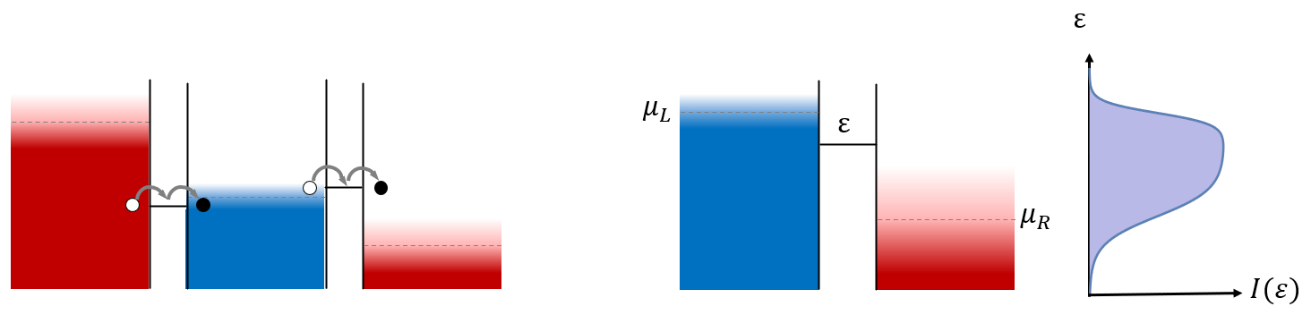
The simplest explanation of the quantum dot refrigerator is that it creates an island of electrons for which only hot electrons can leave and cold electrons can enter. This means that as a current passes through the island, the average temperature of the island is lowered. To be a bit more technical, energy-selective tunneling through quantum dots on either side of the island is used to control the electron flow. An energy diagram illustrating this is shown in figure 1.
Temperature Probe with Heating Channel
To measure the temperature of a quantum ensemble of electrons, one must determine the energy distribution of the particles and fit it to the Fermi-Dirac distribution. For electrons in a 2DEG there are two established ways of measuring the distribution. The first is to measure the current while sweeping the dot's energy level through the Coulomb-blockaded regions as shown in the figure below [3]. The second is to have a dot singularly connected to the reservoir of interest and use a charge-sensing dot to measure the probability of the dot being occupied at different energy levels [4]. The device we designed will be able to utilize both methods, while also using a heating channel to modify temperatures on one side of the dot.
Figure 1
Basic energy-level diagrams to illustrate the working principles of the QDR ( left ) and temperature probe (right ). In these diagrams, energy is represented with the vertical axis and the fullness of the colors is proportional to the probability that a state at a given energy level is filled. Following the electron path from left to right in the QDR design we see: an electron may tunnel from the left lead to one of the lowest energy states in the island while another electron from one of the hottest island energy states can tunnel through the right dot to other lead. In the temperature probe diagram, we show the current through the dot as a function of the dot's energy level, ε. The current is Coulomb blockaded when ε is too high (low) and for any electrons to enter (leave) the dot. The shape of the current vs ε graph at the boundary of the Coulomb blockaded regions is proportional to the temperature.
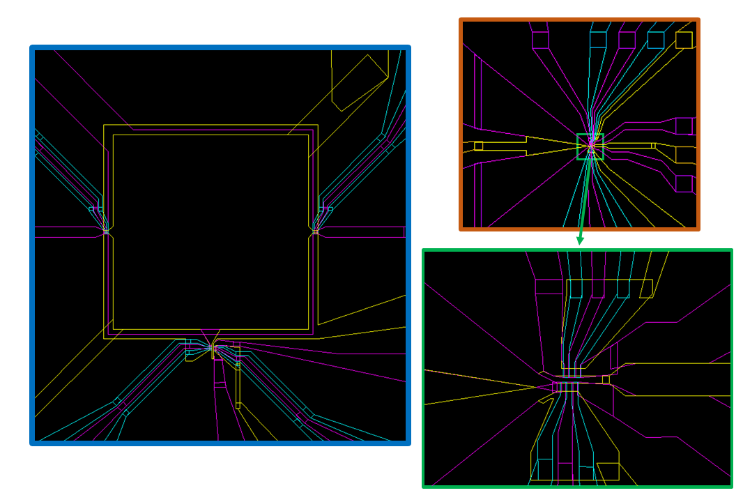
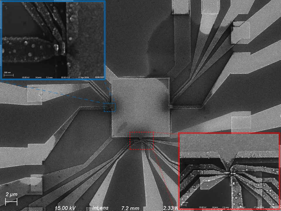
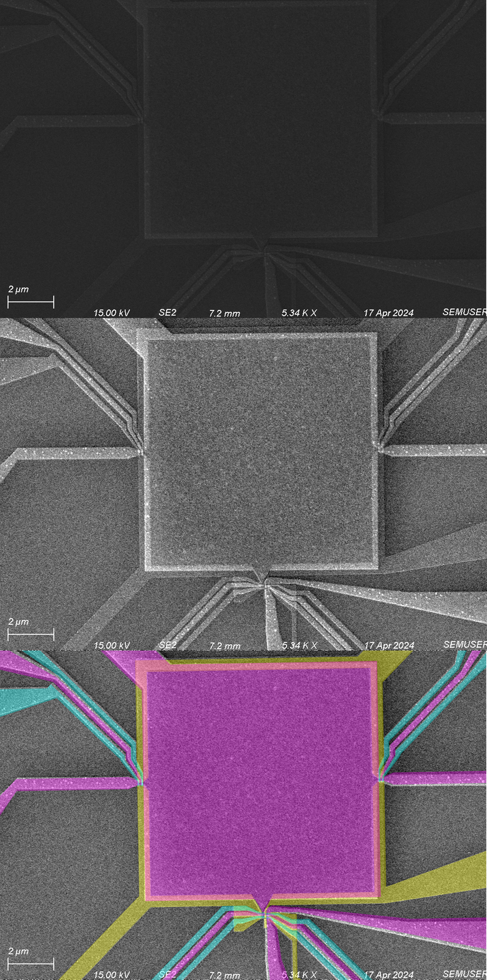
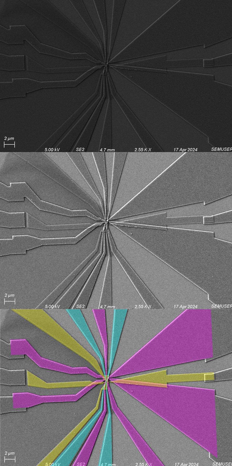
Figure 2
Left: AutoCAD model for the QDR device. Right: AutoCAD models for the temperature probe device at low (above) and high (below) magnifications. The colors represent the different gate layers: screening gates are yellow, tunneling gates are cyan, and the accumulation/plunger gates are magenta.
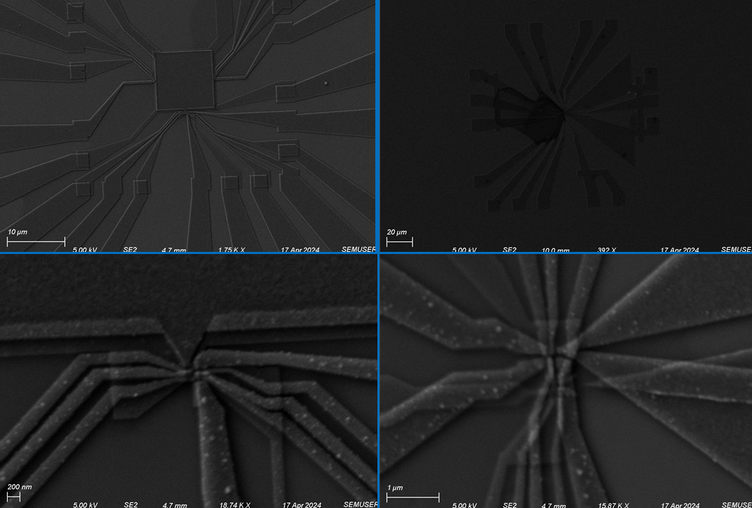
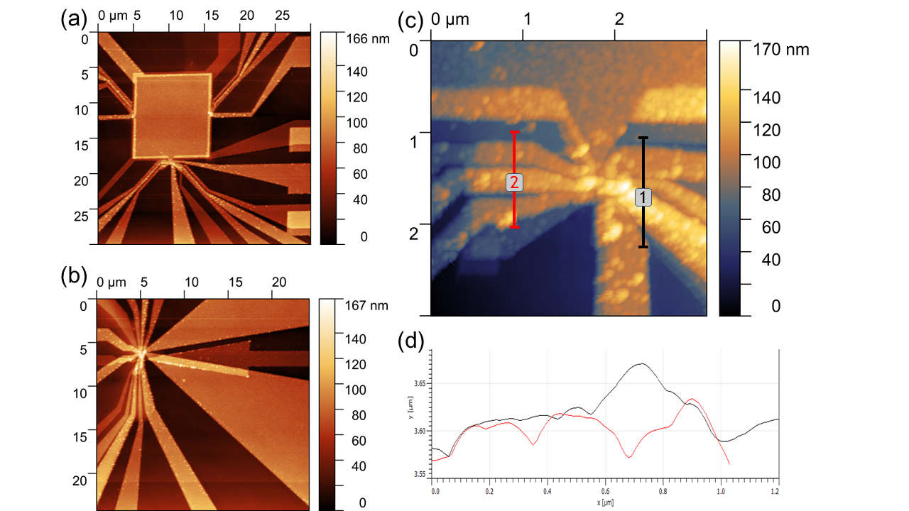
Fabrication
These prototype devices were fabricated on a single chip of undoped Si with three overlapping layers of electron beam lithography (EBL) defined gates. Each layer was created by exposing single layer PMMA resist with 1300 μm/cm^2 with a 100pA beam at 50 kV accelerating voltage. Following exposure, the resist was developed in MIBK:IPA 1:3 and had an aluminum film sputter coated on top. The thickness of the Al screening, tunneling, and accumulation/plunger gates are 30, 50, and 70 nm respectively.