Final Project Report: Scanning Electron Microscope Analysis
Author: Jiheng Duan
Affiliation: Department of Physics and Astronomy, University of Rochester, New York 14627
Email: jiheng.duan@rochester.edu
Introduction
Gate-defined semiconductor spin qubits are subject to decoherence due to their interaction with the environment and fluctuating subsystems on the substrate, which predominantly introduce phase errors and result in a significantly high pure dephasing rate. The short dephasing time limits the fidelity of qubit operations and the performance of spin qubit quantum processors. Recent research suggests that high-fidelity quantum operations can be achieved by precisely shaping pulses, shortening gate times, designing dynamic correction gates, and employing dynamic decoupling protocols. However, balancing fast control with scalability remains challenging. For instance, micromagnets are needed to generate a magnetic field gradient in Si-based single spin qubits to split the single spin state with different Zeeman energies, which separates the pulsing frequency for fast electric dipole spin resonance (EDSR)-based single-qubit control. Conversely, ST qubits, which encode logic 0 and 1 using a two-spin state formed by adjacent quantum dots, require only a homogeneous global magnetic field and promise better scalability. However, their single-qubit operations can only be approximated by biasing three static gate electrodes, leading to a more limited degree of freedom for rotation on the Bloch sphere and longer gate times than those of EDSR.
In this work, we present a partial fabrication process for a four-dot Si-based quantum processor. We anticipate significant challenges, including fabricating a functional spin qubit, minimizing charge noise levels by depositing clean top gates, and maintaining a low misalignment threshold during electron beam lithography (EBL). We plan to document the entire process, starting with a diced 6mm 6mm Si/SiGe wafer. We will analyze the fine structure of confining gates using a scanning electron microscope (SEM) and determine the optimal auto-alignment strategy on Elionix. Large features such as bond pads, on-chip connection lines, and global alignment marks are fabricated by a laser writer and proceeded with depositions of aluminum or gold. Furthermore, we will characterize the surface using InLens and secondary electron imaging. Additionally, we will conduct backscattered imaging and X-ray analysis at high magnification to ascertain the presence of any small metal fragments or surface impurities introduced during the fabrication process, which could potentially serve as sources of charge noise. Resulting images will be analyzed using ImageJ and colored by Photoshop. This project aims to deepen our understanding of the intricacies involved in quantum dot fabrication and strategies for reducing noise in sample fabrication.
Device Fabrication
The substrate of this sample is from University Wafer II, diced and cleaned at URnano. As nano-scale quantum dots cannot be directly wire-bonded to a PCB board, a layer of macroscopic features must be patterned and deposited using optical lithography and a thermal evaporator. As shown in Fig. 1, we define the bond pad, on-chip connection lines, and global alignment marks at URnano by spin-coating a layer of AZ5214e-IR photoresist and exposing it with a negative tone recipe using a laser writer. After developing and cleaning the pattern with MF319 and a plasma cleaner, the patterned chip is loaded into the thermal evaporator in Nichol lab and 3/80 nm Cr/Au is deposited. The thin layer of chromium helps the gold adhere to the silicon chip, and the deposited gold allows the chip to be easily imaged by backscattered electron in both SEM and Elionix.
Misalignment is one of the most significant issues limiting the functionality of such nano-scale multi-layer quantum devices. As macroscopic features scale around several micrometers, they are not accurate enough to align nano-scale gate electrodes. Consequently, smaller local alignment marks are naturally required to achieve high-precision alignment, using the global marks and fabricated by Elionix. After being spin-coated with polymethyl methacrylate (PMMA), the chip is loaded into Elionix and prepared for exposure.
To establish better beam conditions, a pre-set of well-tuned beam configurations is recalled, featuring optimal beam current and other parameters. To achieve better focus, on top of autofocus-stigmatism and dynamic focus, a set of contamination dots is made by employing spot mode of the electron beam until a clean donut-shaped exposed dot can be observed. Finally, after confirming the schedule file (including alignment mark search, dose time, beam current switching), the chip is ready for the process.
By repeating this process (being careful to increase the searching area of both local and global alignment marks and adjust to the optimal dose time for the current layer), well-aligned quantum dots can be successfully patterned.
After EBL patterning the local alignment marks, the chip is loaded back into the thermal evaporator and coated with 3/80 nm Cr/Au. For the subsequent layer of gate electrodes, the chip is loaded into the electron beam evaporation system in Nichol lab and deposited with 30 nm (first layer) and 50 nm (subsequent layers) of Al, manually with a 5 nm buffer layer.
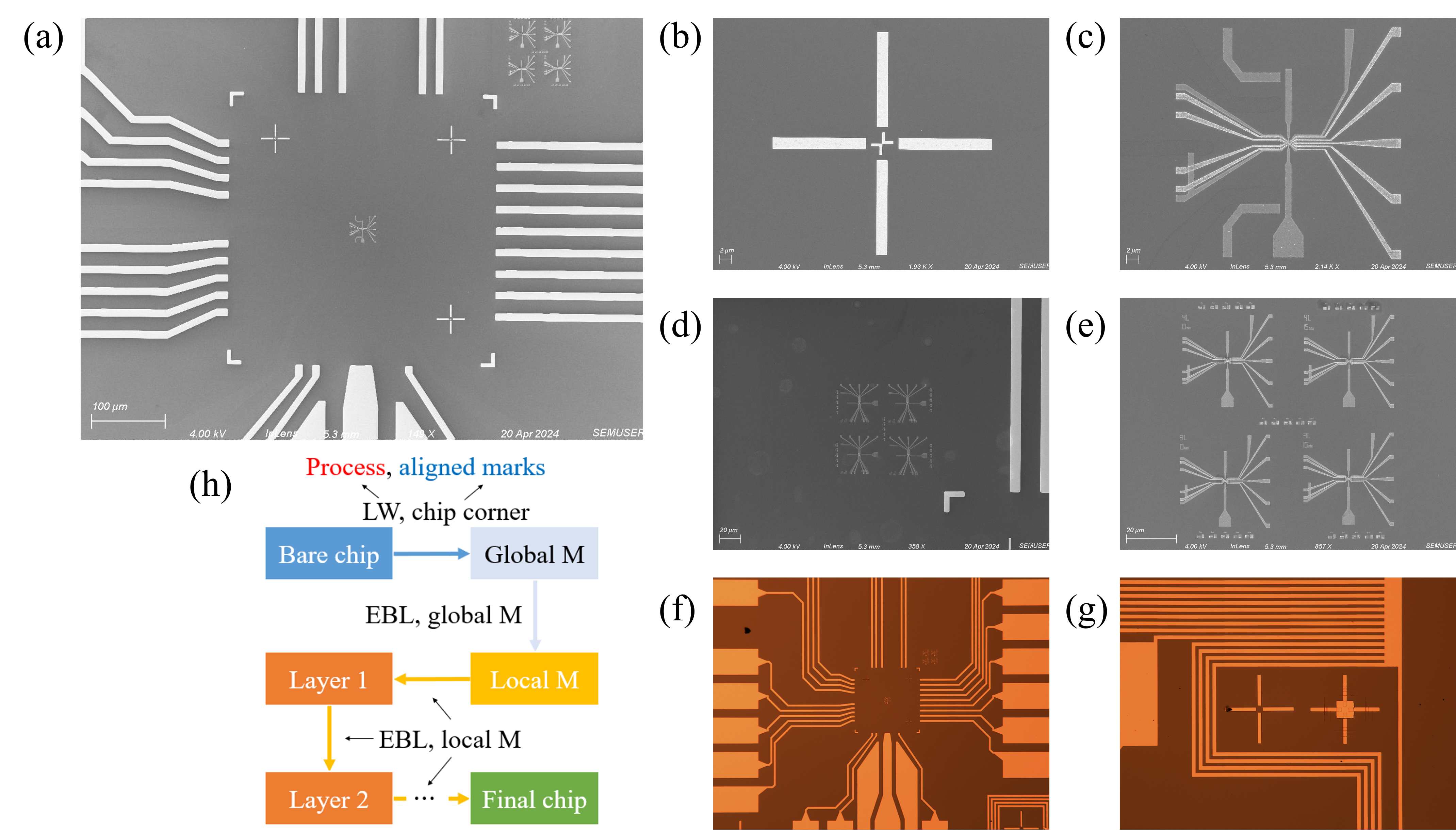
Figure 1. Macroscopic features. (a) Overview of the dot region. (b) Local alignment mark. (c) Zooming into the dot region. (d)-(e) Test patterns. (f) Optical microscope image of the dot region. (g) Optical microscope image of the global alignment marks. (h) Detailed lithography workflow, M: marks, EBL: electron beam lithography, LW: laser writer.
Imaging Results
We image using an optical microscope and an InLens detector in SEM. We chose not to use Secondary Electron 2 (SE2), Backscattered Electron (BSE), and Characteristic X-ray imaging because (a) SE2 and BSE both miss parts of surface information as each layer of gate electrode is only about 50 nm thick and (b) it is very difficult to collect the diffracted X-rays from the Al thin film on the surface of the substrate. An interaction volume simulation is shown in Fig. 2, where the accelerating voltage is 4 kV. In the most ideal case, the electron beam penetrates down to the SiGe substrate, meaning the volume regions for SE2 and BSE are too deep to affect the surface. Also, the collected X-rays mostly originate from the substrate, making it extremely difficult to detect any small pieces of Al thin film on the substrate's surface.
In the following section, we primarily present the results obtained from the InLens detector with an accelerating voltage set at exactly 4 kV and a working distance of about 5.3 mm.
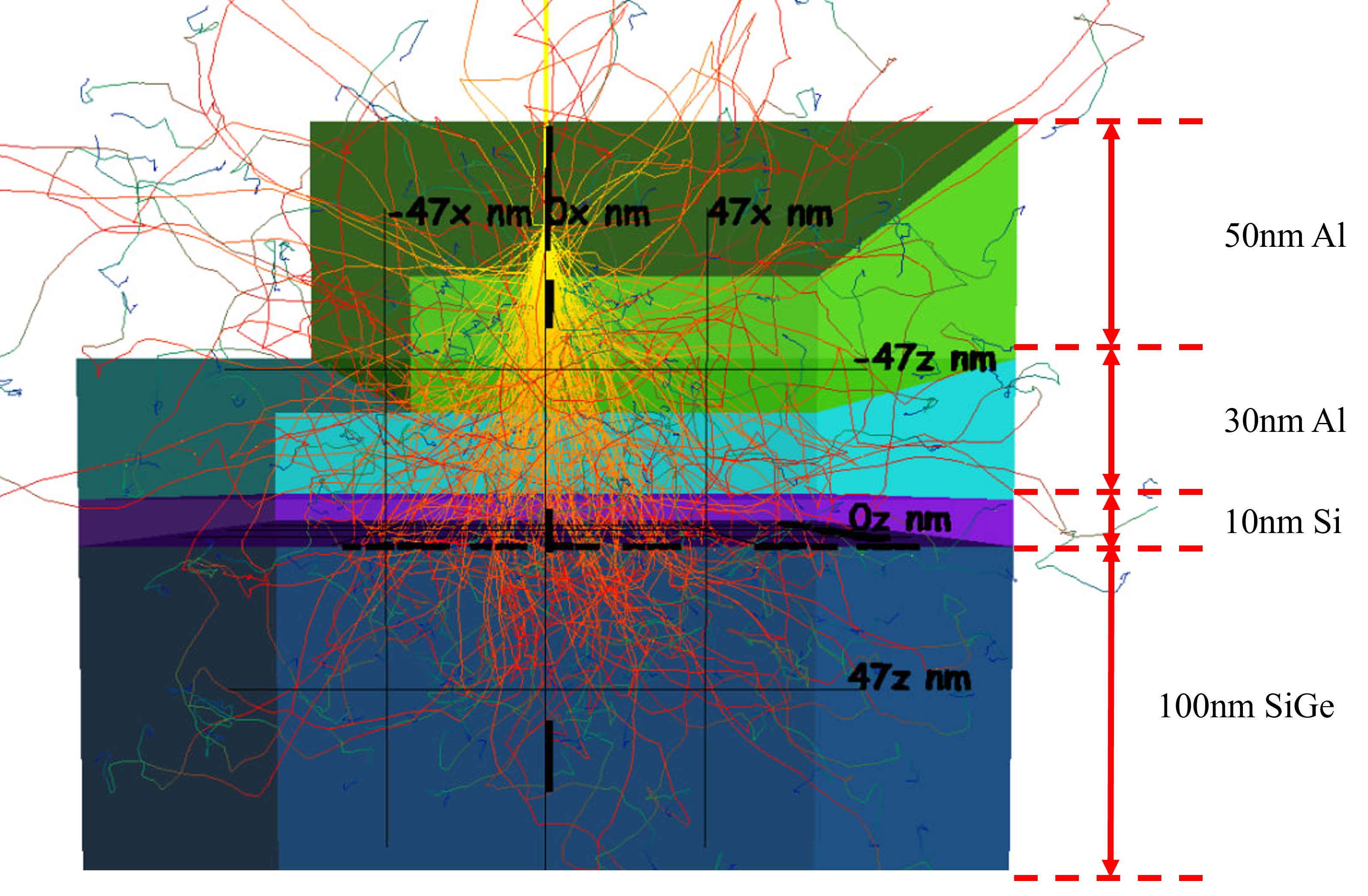
Figure 2. Interaction volume modeling. The simulated accelerating voltage is 4kV. The sample is modeled as the realistic device with two layer of aluminum with different thickness, a silicon cap sandwiched by aluminum and 100nm silicon-germanium substrate.
Dose test
E-beam lithography operates by directing a focused electron beam onto specific regions of a sample that has been coated with a PMMA resist layer and breaks the chemical bonds in the exposed region, making the PMMA removable by a solvent developer. Due to variations in the geometry of patterns across different layers, the optimal dose—measured in and indicating how many electrons per unit area are needed—varies, resulting in a proximity effect. Therefore, conducting a dose test on a dummy silicon chip to ascertain the ideal doses for various layers is necessary to enhance the efficiency of subsequent EBL processes, such as the removal of excess metal. The design of the current device incorporates four distinct layers, all merged into a single CAD file to streamline the dose testing process. As the fabrication includes only the first two layers, we have recorded only the corresponding optimal doses, shown in Table 1.
Table 1: Description of the Table
| Layer index | Name | Optimal Dose () |
|---|---|---|
| Layer 1 | Accumulationc& screening gate | 1300 |
| Layer 2 | Barrier gate | 1720 |
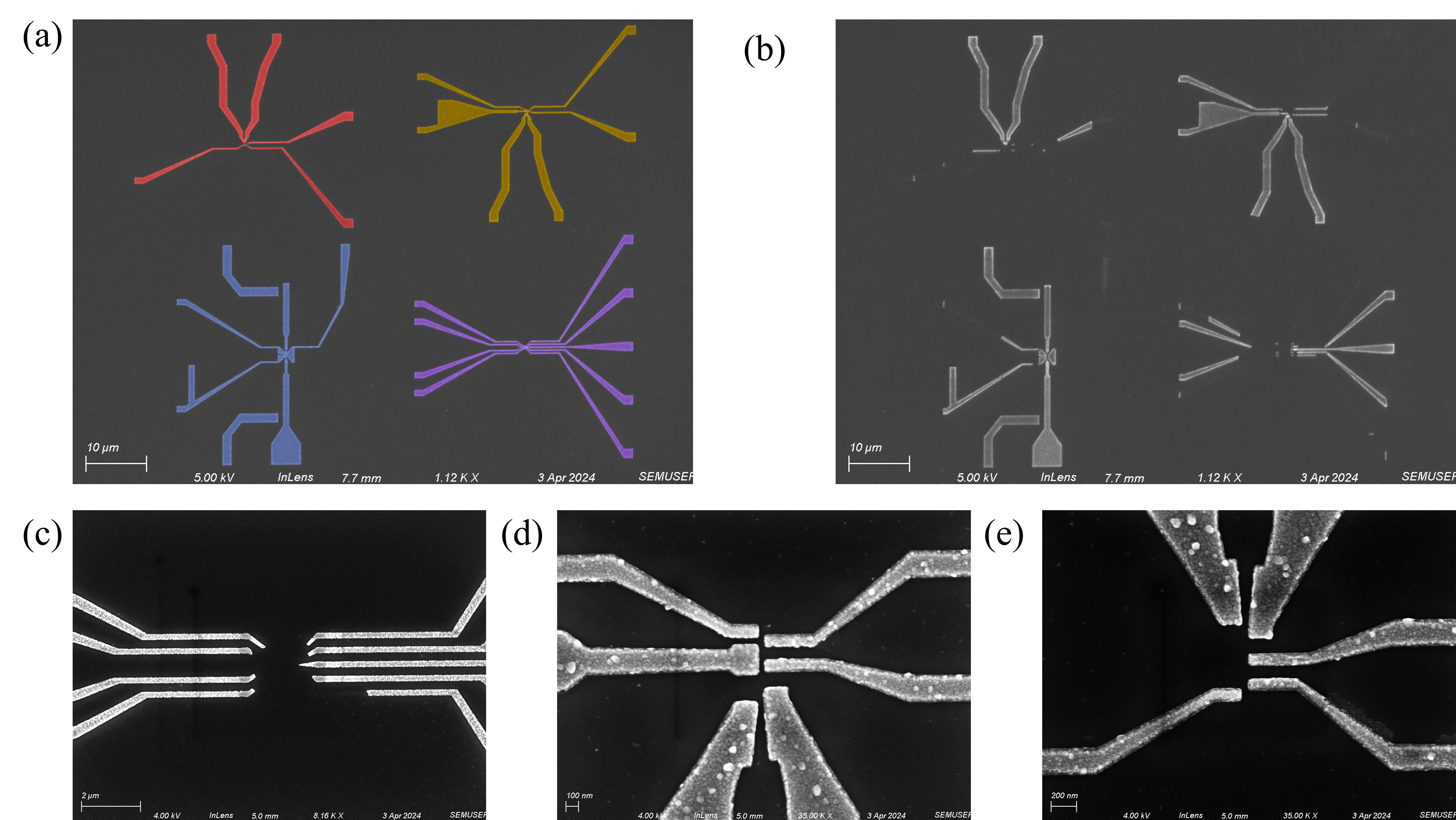
Figure 3. Dose test images. (a) Four-layer structure in good dose. (b) Poor dose case. (c)-(e) Zooming into poor dose case.
Two-layer alignment
We observe a global misalignment effect on the device, as shown in Fig. 4, where the second layer barrier gate is collectively shifted to the left.
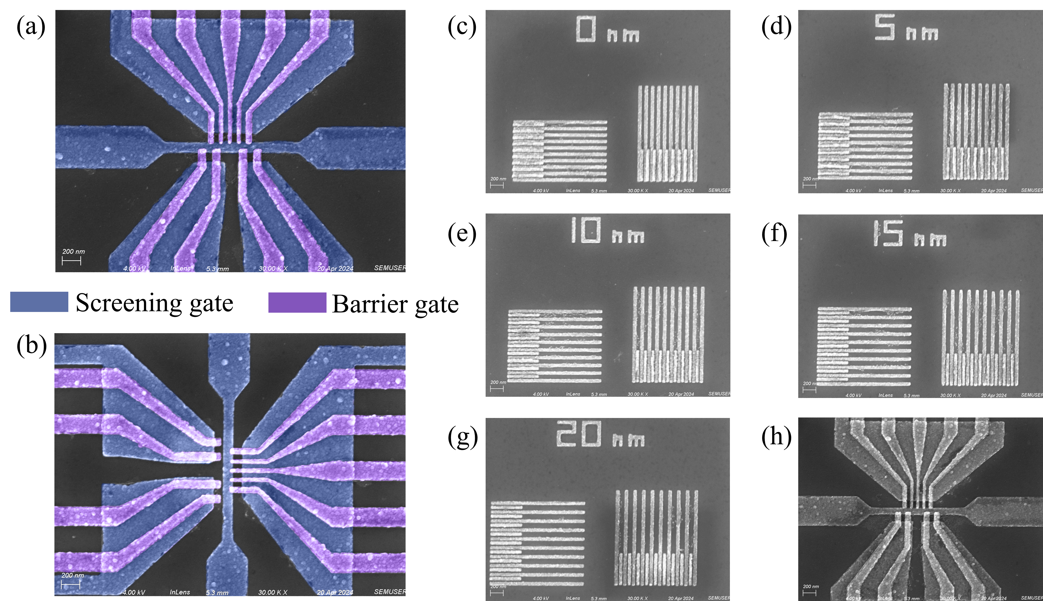
Figure 4. (a)-(b) Miss alignment on the direction. (c)-(g) Miss alignment test with different spacing. (h) Relative good alignment without coloring.
Residual PPMA
Fig. 5 shows some residual PMMA on the substrate, which may be due to insufficient lift-off (LO).
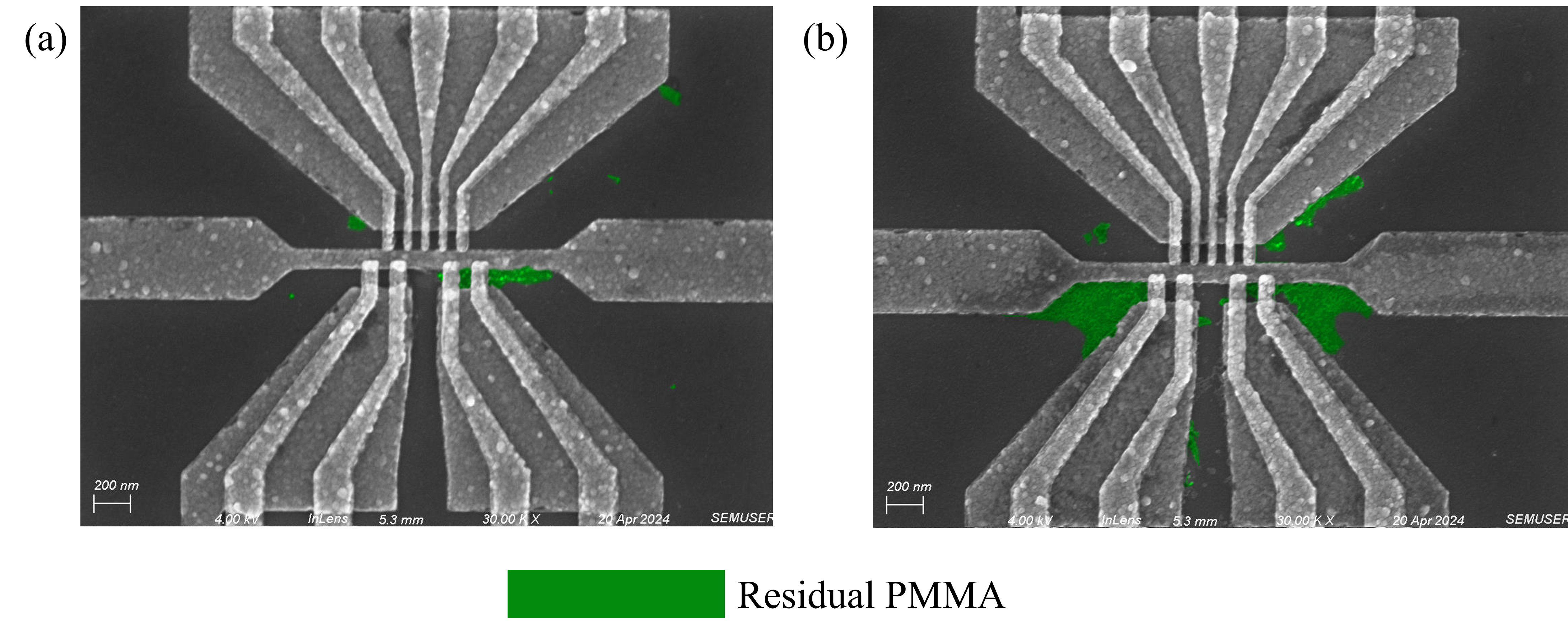
Figure 5. Residual PMMA due to insufficient lift-off.
Conclusion
We have finalized the optimal dose for each layer of the device. The auto-alignment on Elionix is still imperfect. Some residual PMMA observed on the chip indicates issues with the lift-off (LO) process.
Acknowledgement
The Author would like to thank Feiyang Ye and Jacob Markowski for their help with device fabrications. Thanks to Sean O’Neill and Gregory Madejski for their help on EBL and SEM training. Thanks to John Nichol for authorizing the Si-QD4 design.