Table of Contents
- Introduction
- Fabrication
- Light Microscopy (LM)
- Electron Beam Lithography (EBL)
- Scanning Electron Microscopy (SEM)
- Colorizations
- Image Analysis
- Acknowledgements
- References
Introduction
Electron-beam-lithography (EBL) implements a focused beam of electrons to write nanoscale patterns on electron-sensitive substrates. The proximity effect is caused by electrons scattering off resist material as it is exposed under a focus electron beam. This can compromise the accuracy of structures as it generates unintended exposures and additional dosage to pre-exposed patterns. Correction of the proximity effect in EBL is important for the nanofabrication of quantum devices, as it can mitigate distortions and allow for high-resolution. Existing techniques for mitigating proximity effects include dose modulation, shape modification, and computational correction algorithms. Dose modulation adjusts the intensity of the electron beam based on the proximity of neighbor features. This project implements dose modulation for direct measurement of resolution limits in EBL. Which can be used to optimize exposure dose distribution to compensate for electron scattering.
Fabrication
Fabrication processes adapt according to the specific sample and experimental objectives. Preparing samples for electron microscopy and lithography involves crucial steps to maintain their structural integrity and surface details.For this project, a silicon (Si) chip was cleaned with IPA and acetone, followed by nitrogen gas drying. Subsequently, a drop of PMMA (polymethyl methacrylate) was deposited onto the chip's surface, which was then uniformly spread through spinning. Afterward, the chip underwent a ten-minute baking session to optimize the resist's properties. A small scratch was etched onto the surface of the chip, to indicate the area where the EBL would subsequently make a pattern
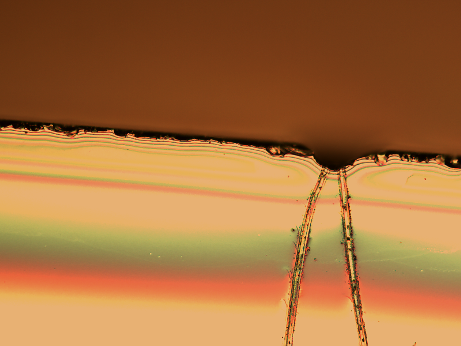
Figure 1: LM image of Si chip, post PMMA.
Prior to sputter coating, the chip was mounted onto a metal stub using double sided carbon tape, to increase conductivity. This experiment used a Platinum (Pt) direct current sputtering system to coat the chip. Coating a sample with Pt, an electrically conductive material, prevents charge build up from forming at the surface, while increasing the emission of secondary and backscattered electrons. Through the sputtering process an ultr-thin-layer ~6nm of Pt is deposited evenly on the chip’s surface. Techniques like sample coating further mitigate charging effects by altering the interaction volume to enhance image quality.
Light Microscopy (LM)
Light microscopy (LM) was employed for both quality control and rapid examinations throughout the fabrication process. Initial inspections were conducted under LM to evaluate the sample's condition prior to EBL exposure. Between fabrication stages, LM was utilized to confirm the resist coat on the chip was uniform and uncontaminated. These observations guided the selection of the exposure area. Following resist exposure, LM allowed for examination of the features generated by EBL.
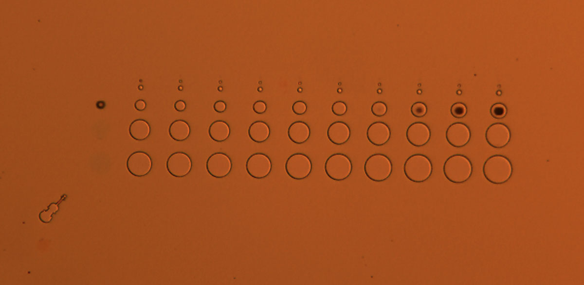
Figure 2: LM image of full EBL expoused pattern
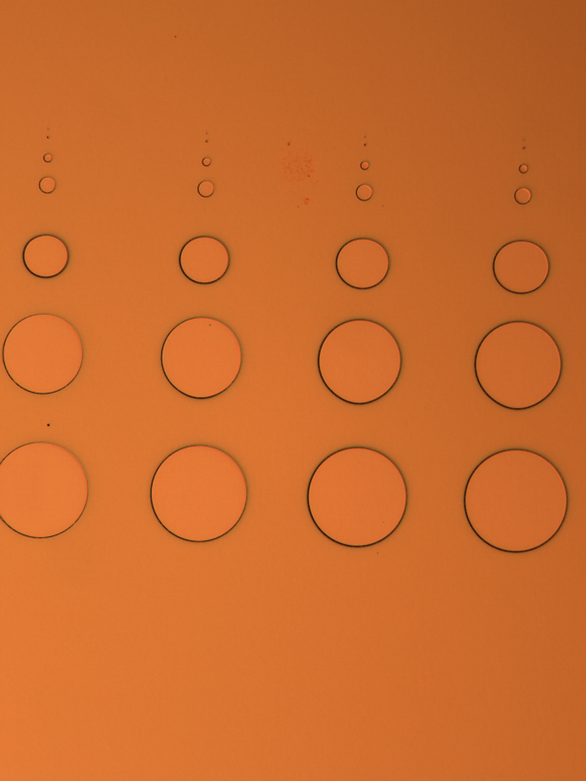
Figure 3: LM image of patters with increasing dosages from left (of 750μC/cm^2, ) to right (2250μC/cm^2).
Electron Beam Lithography (EBL)
The pattern exposed under the EBL was composed of 11 lines. Each line was made up of 11 points with diameters ranging from 2nm to 50μm. Each line was given a dose that was 500μC/cm^2 higher than the previous one. The lowest dose give was 250μC/cm^2 and the highest does given was 5250μC/cm^2.
Figure 4 shows the exposed pattern, where the dosage decreases from left to right. The red column has the lowest dosage 250μC/cm^2 , the orange, yellow, green, and blue columns have dosages of 750μC/cm^2, 1250μC/cm^2 , 1750μC/cm^2 , and 2250μC/cm^2 respectively.
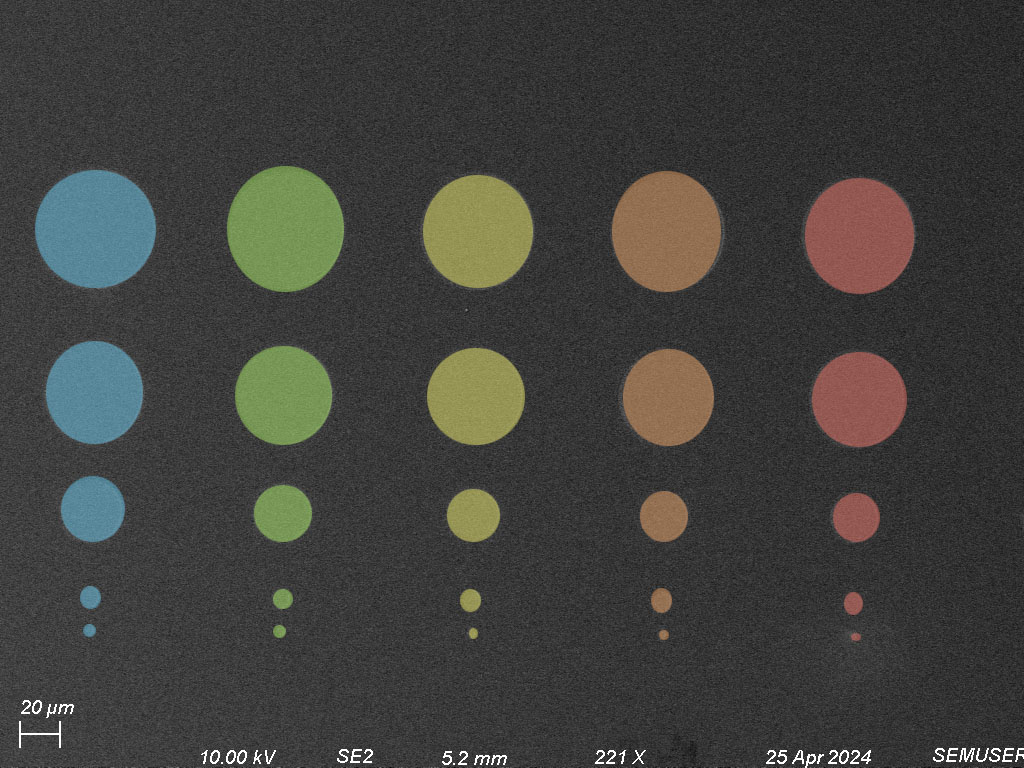
Figure 4. Colorized SEM image of point exposures.
Scanning Electron Microscopy (SEM)
Scanning electron microscopy (SEM) offers a diverse array of imaging modes, each tailored to specific sample characteristics and analytical objectives. SEM was used to image the Si chip after EBL exposure.
Finding small scale features is oftentimes challenging. This can be facilitated by adding a larger, and distinguishable feature to the exposed pattern. Violins were instrumental for locating point structures within the sample.
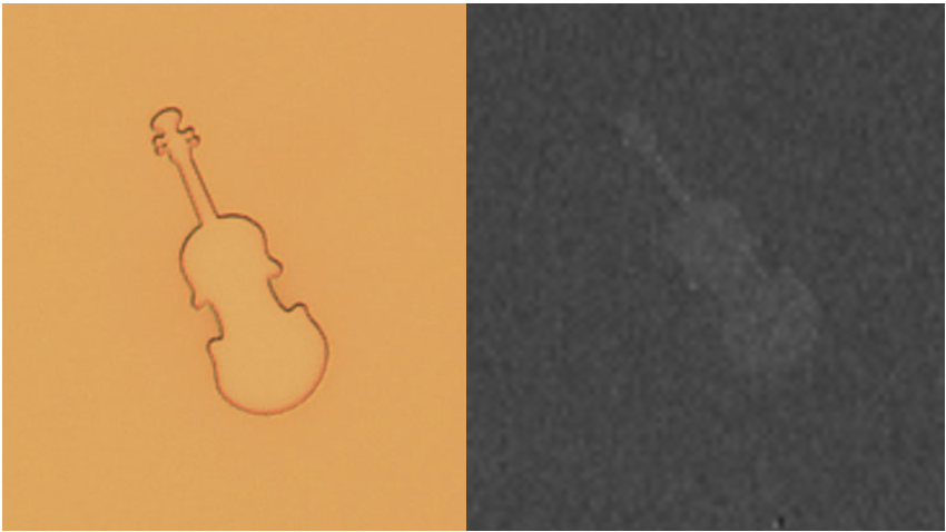
Figure 5: Reference violins.
SE2 Detector

Secondary electron (SE) imaging detects electrons emitted from a sample’s surface in response to exposure from the electron beam. This imaging mode is particularly useful for surface analysis as it highlights surface features, revealing details such as roughness and texture with clarity and resolution. A SE2 detector was used to image the chip with an accelerating voltage of 10 keV.
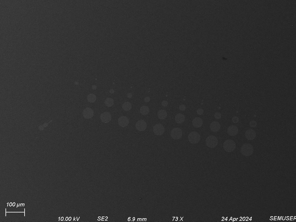
Figure 7: SE2 image of full exposure pattern.
In-Lens Detector
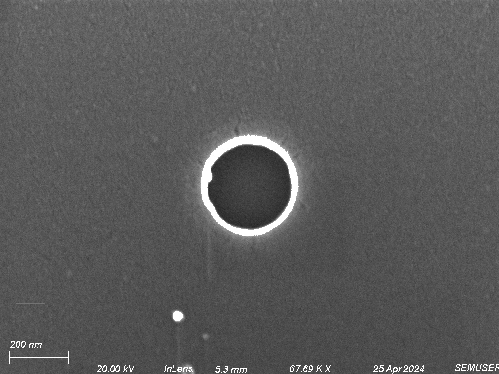
In-lens detectors generate and amplify signals generated by electrons interacting with a sample’s surface. Thus, in-lens is a great tool for obtaining topological information from samples. An in-lense detector was used to image the sample with accelerating voltages of 10kV and 20kV.
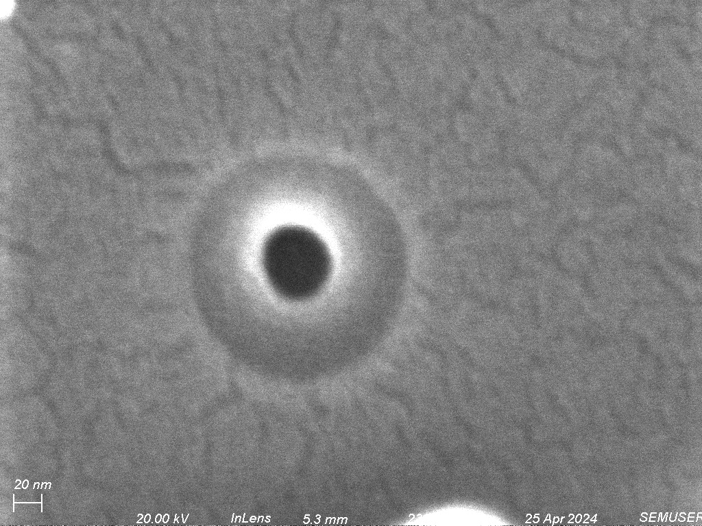
Figure 9: In-Lense image of (5250μC/cm^2)feature with d = 50nm, with brightness & contrast enhancement
Colorization
Adobe Photoshop, and ImageJ were used for colorization of the SEM images. Colorization makes it easier to identify key features within the images, like the outline and diameter of each point.
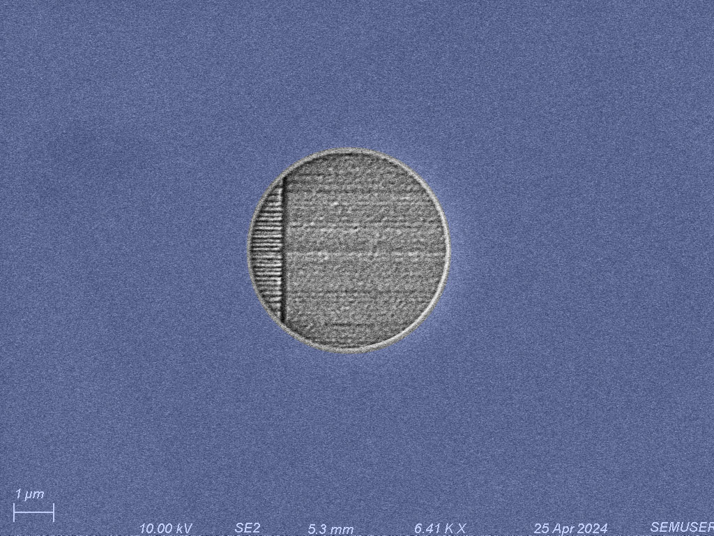
Figure 10: Colorized SEM image
Image Analysis
Visualization of the point exposure with a 50nm diameter was only achieved at the two highest doses (5250μC/cm^2, 4750μC/cm^2). The lowest dosage to properly expose the 100nm diameter point was visible at dosages as low as1750μC/cm^2.
Dark squares found in the images are a result of organic debris present on the sample’s surface, which can volatilize when exposed to the electron beam and recondenses, forming a carbon buildup. This phenomenon becomes more pronounced at higher accelerating voltages, since increased energy enhances the volatizarían of organic matter.
Acknowledgements
I would like to thank Sean O’Neill and Gregory Madejski for their guidance throughout this project
References
Rishton, S. A., and D. P. Kern. "Point exposure distribution measurements for proximity correction in electron beam lithography on a sub‐100 nm scale." Journal of Vacuum Science & Technology B: Microelectronics Processing and Phenomena 5.1 (1987): 135-141.