University of Rochester, Institute of Optics
Goal
The goal of this project was to locate the same Upconverting Nanoparticles (UCNPs) whose luminescence was observed using our optical microscope and APD detector, in both the Scanning Electron Microscope (SEM) and Atomic Force Microscope (AFM). Then, using the Transmission Electron Microscope (TEM) and ImageJ analysis, the diameter of the particles was determined.
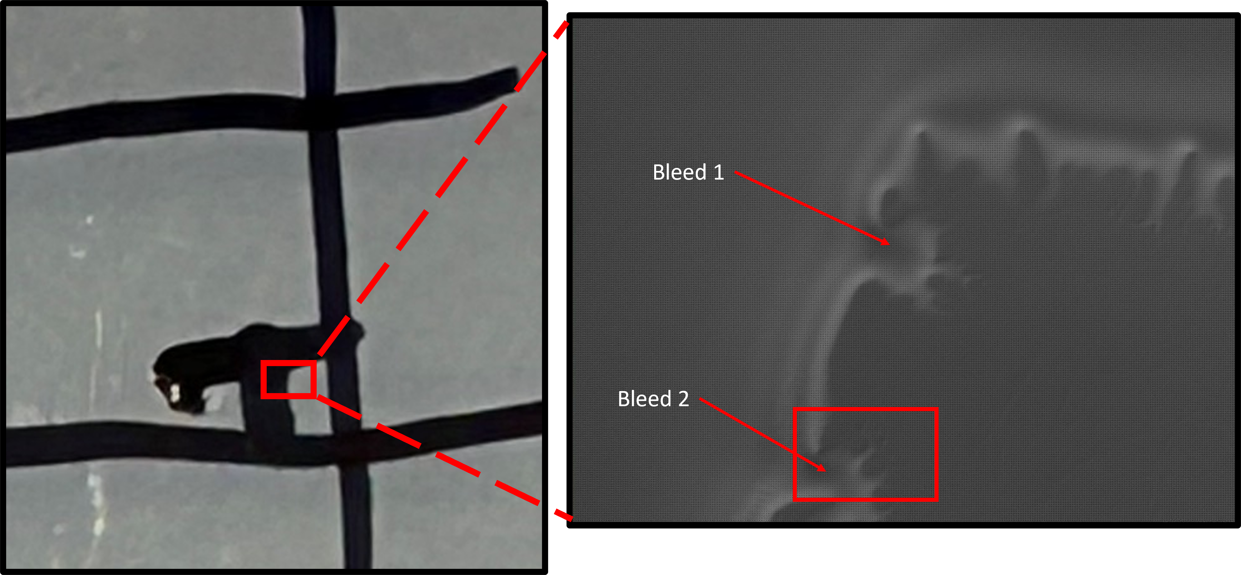
1. IntroductionOur research, under advisor Andrea Pickel, consists of optically imaging the luminescence of individual UCNPs on a glass substrate and using ratiometric luminescence thermometry to determine the temperature at the nanoscale (1). Fiducial markers are used to find the same location of a sample repeatedly however, there are no optically transparent substrates with fiducial markers that are conductive, which is required to view them in the SEM and optical microscope. Instead, an SEM pen was used to hand-draw fiducial markers in the shape of a pound sign and a T. This pen is unique because the ink is made of a conductive material, carbon, which makes it easily viewable in the SEM. The fiducial marker used for finding the same set of nanoparticles was the inside corner of a T which can be seen in Figure 1a and is further magnified in Figure 1b. Since the fiducial marker is visible in the SEM, these marks are used to find the location of interest. Thus, allowing the identification of if the luminescence seen is from single or multiple UCNPs.
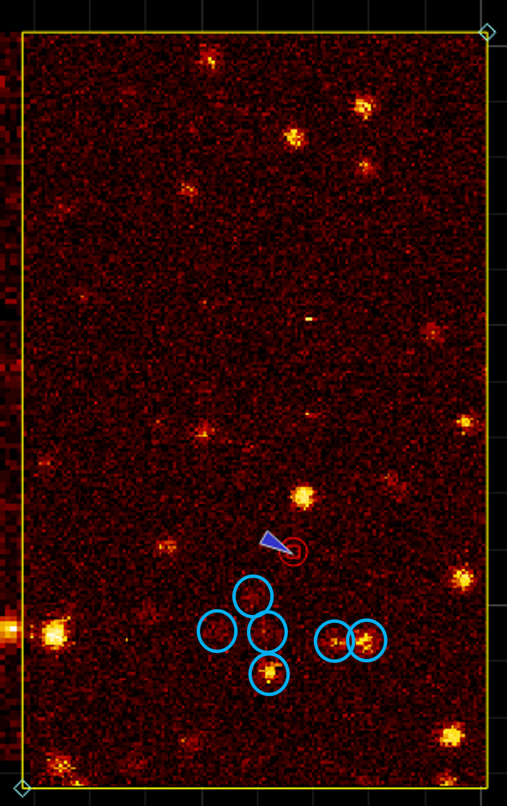
UCNPs are given their name of upconverting as they absorb at 980 nm infrared light and emit ~550 green light. Athough this is decreasing in wavelength, this is an increase in energy. Nd3+ doped with Yb3+ and Er3+, was the UCNPs used for this experiment. Nd3+ ions absorb two 980 nm photons and transfer energy to the Yb3+ and ultimately excite the Er3+ ions, which then emit in the visible wavelength range (1). UCNPs are advantageous as they enable optical non-contact thermometry meaning that there isn't parasitic heat sinking from contact with the sample to affect temperature measurements. For our reseach, we use them for elucidating thermal contributions in plasmonic photocatalysis. Figure 2 shows an example of what we would see in our APD detector. It can be misleading to just look at the luminescence map to identify single particles, which is why the SEM is required.
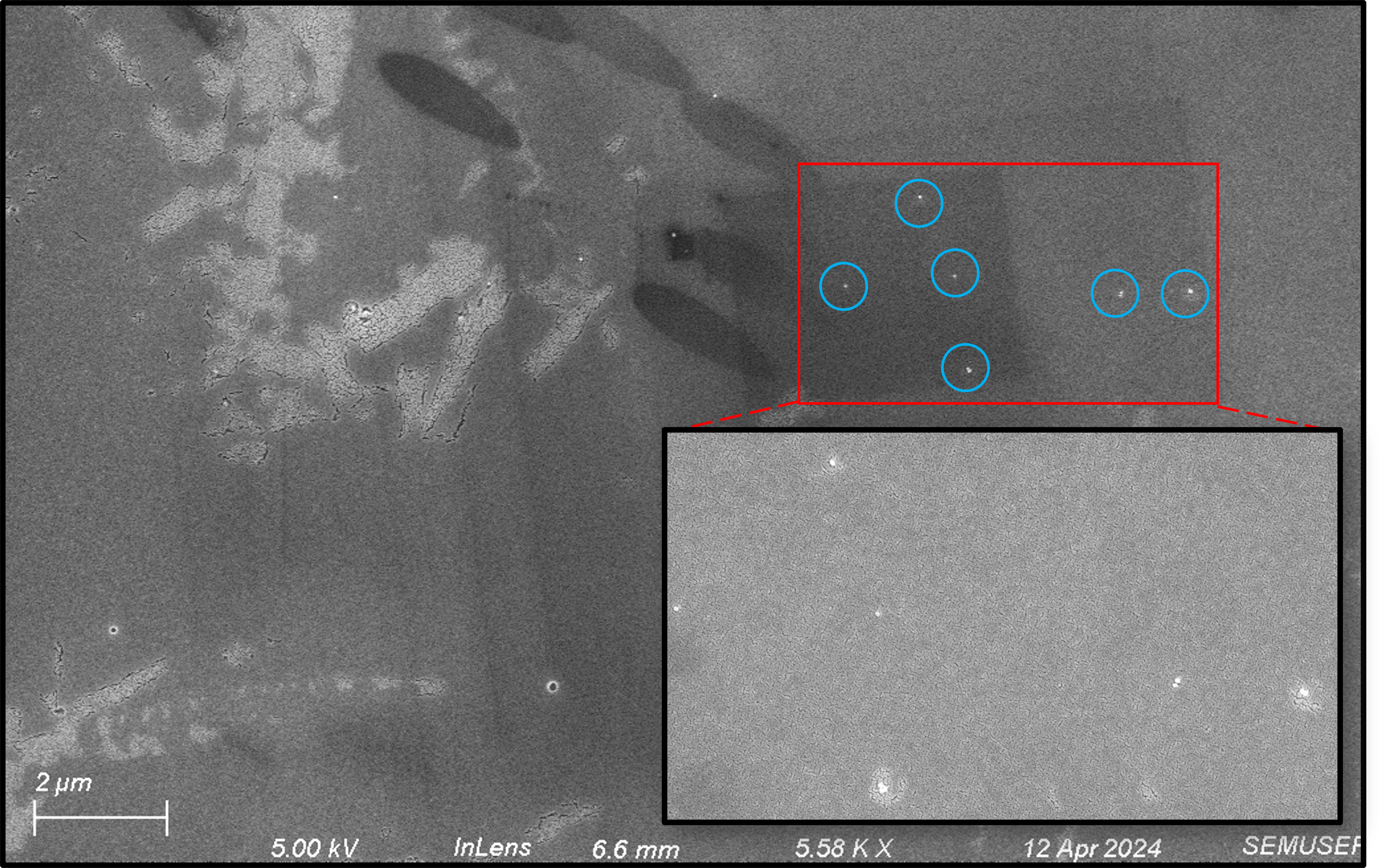
Using the APD, we were able to complete a large scan of an area near the second pen bleed seen in Figure 1b. From the number of photon counts detected by the APD for a particular spot, we can identify the NPs we suspect are individuals from those that most likely are not. We chose a unique pattern of NPs to identify in the SEM as we thought it's uniqueness would aid in the repeatability of finding the NPs. The chosen pattern represents a cross type shape and can be seen in Figure 2.
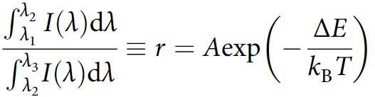
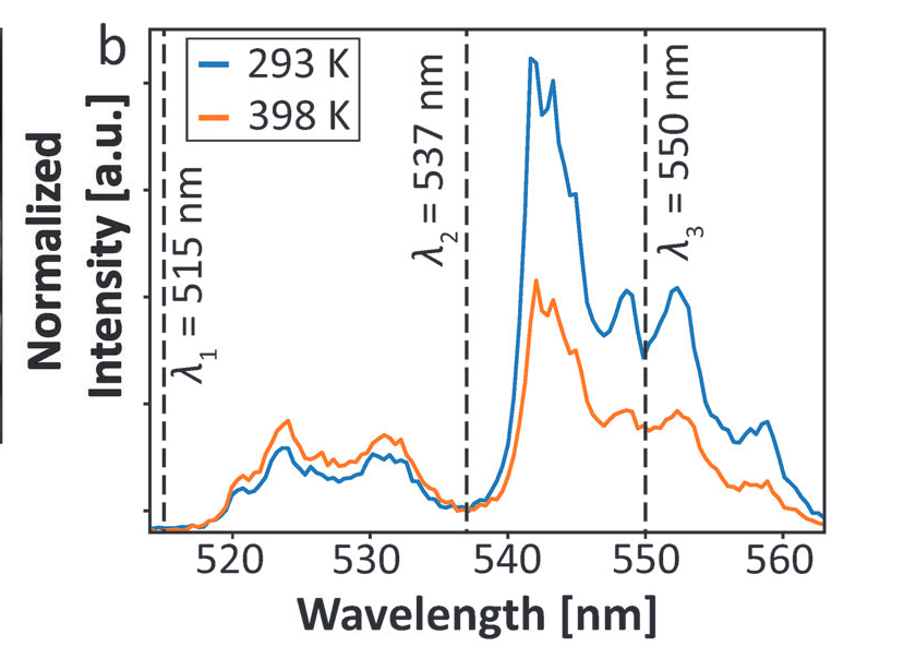
Ratiometric thermometry is the most popular way to measure temperature using NaYF4:Yb3+, Er3+. The Er3+ is excited and decays non-radiatively to its 2H 11/2 and 4S 3/2 manifolds. The close spacing of these energy levels gives rise to a temperature dependent luminsecnce. Radiative relaxation from these manifolds to the ground state results in the emission of a single photon in the green wavelength (~515-565). The temperature dependent luminescence can be calibrated using equation 1. We select 𝜆1 = 515 nm, 𝜆2 = 537 nm, and 𝜆3 = 550 nm to exclude the peak that appears near 556 nm due to a known excited state to excited state transition, the physics of which is not captured by Equation 1. (1)
To view our sample in the SEM, we needed our sample substrate, the glass, to be conductive. A gold coating was sputtered onto the sample for 60 seconds, at a rate that corresponds to about 6 nm of gold. A small piece of carbon tape was used to secure the sample to the sample mount, and an additional smaller piece was placed on top to connect the gold coating on the surface to the sample mount. This allows electrons to disperse from the surface. I found 60 seconds to be an appropriate amount as the charging was tolerable while keeping the sample optically transparent. The InLens, which detects secondary electrons (SE2) was used with low accelerating voltage and a short working distance. SE2s were chosen over backscattered electrons or x-rays because SE2s origionate from the top of the sample where the UCNPs reside. The short working distance increases the resolution by reducing the spot size. The low accelerating voltage limits the quantity of electrons irradiating the sample and reduces the interaction volume. The fiducial marker was used to find the cross pattern in the SEM and individual particles could be distinguished.
4. Particle Size Analysis from SEM
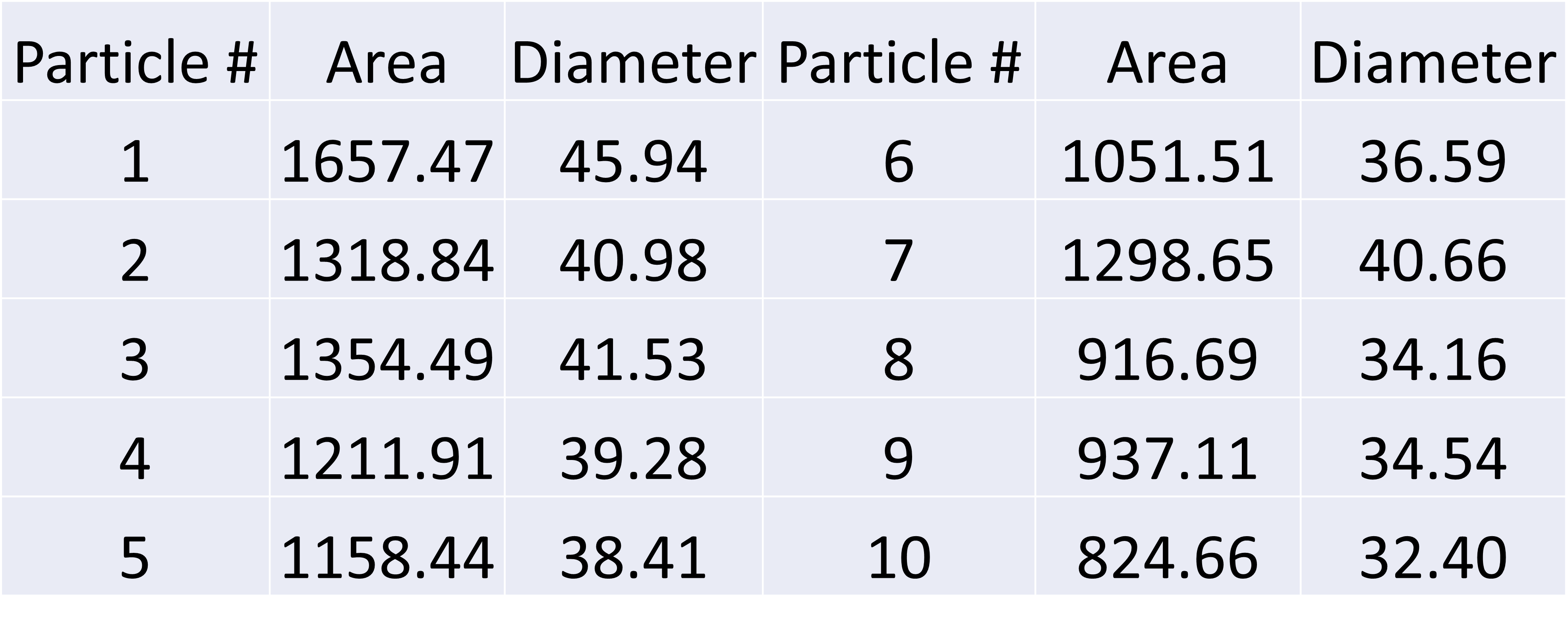
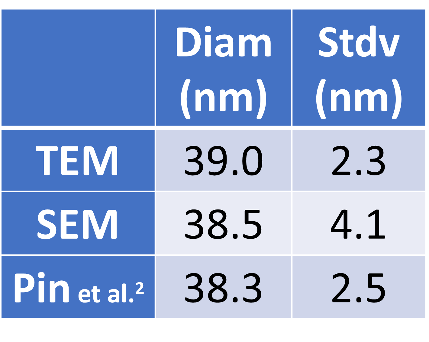
ImageJ software was used to determine the diameter of the particles of Figure 3. To do a particle analysis of the entire image, the following image manipulations were made: subtracted background using a 10 pixel size parabola, enhanced contrast by 1%, the threshold was set from 0-76, despeckled, and watershed to ungroup multiple particles. An analysis of the particle's area ranging of 50-2,000 nm^2 assuming a circularity greater than 0.8 was done. All 10 particles seen in the cross shape fit in these analysis parameters. Note that the manufactured quoted size of the particles is 50 nm in diameter and 2,000 nm^2 corresponds to approximately 50 nm diameter. The results are shown in Table 1. The average particle size measured was (38.45±4.10) nm. Thus the 50 nm reported size does not fit in our measured data. I suspected that this might have been a result of the manipulations that I made in ImageJ, the reduced resolution that the SEM has compared to the TEM, or that the sample size of 10 NPs was too small. This inspired a separate analysis of particle size in the TEM with a higher concentration of UCNPs.
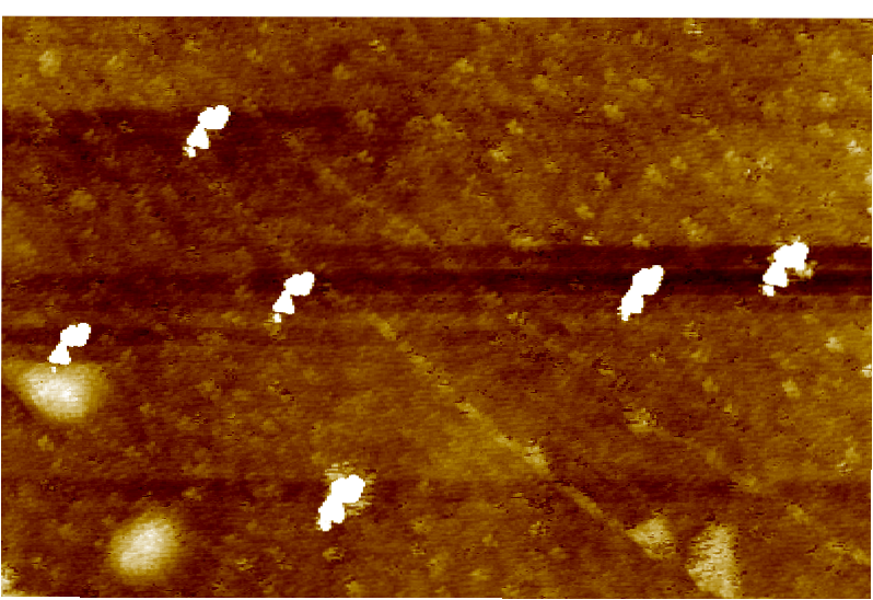
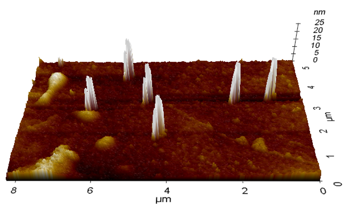
Our lab’s personal AFM was used to detect changes in height to find the same NPs found in the APD and the SEM. A non-contact tip was used. The fiducial marker was visible from the optical microscope in the AFM and used to get a high-resolution scan of the NPs of interest. Even at the highest resolution scan, the individual particles cannot be determined.
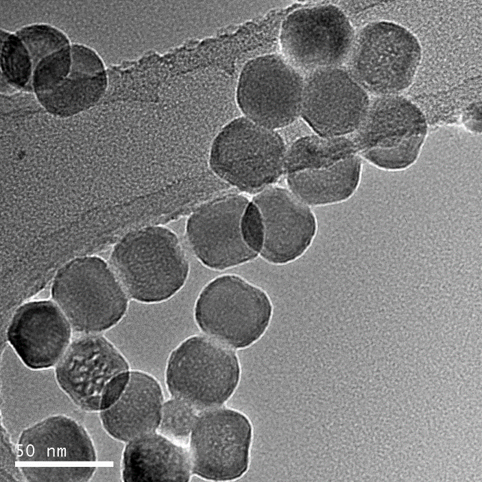
To reanalyze the particle size, a larger concentration (1/10 of the UCNPs original concentration) of NPs was drop casted on a TEM ultra-thin carbon support grid. The TEM images were taken under bright field imaging conditions. To maximize the image contrast, the image was set to be slightly underfocused. Several images were taken at different locations to ensure a representative sampling of the particle size, instead of just a few NPs as was done with the SEM. The images were analyzed using ImageJ where each particle was fitted with a circle and measured individually. The results reporting an average particle diameter of (39.01±2.29) nm. This is consistent with our measured SEM data and Pin et al. (2) but does not contain the quoted 50 nm. The results can be seen in Table 2.
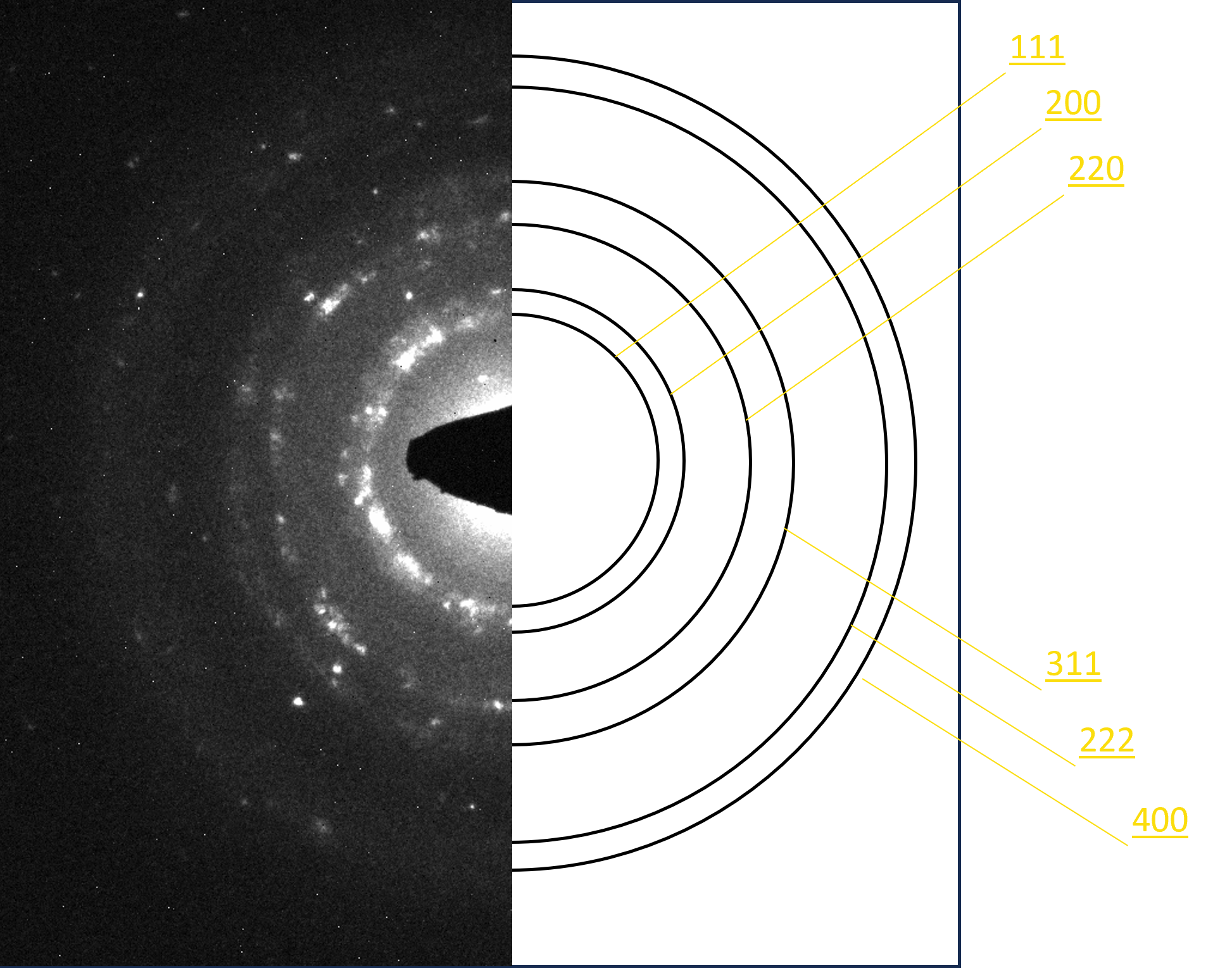
Then the TEM was switched to diffraction imaging. The selected-area electron diffraction (SAED) pattern from the NPs showed a ring pattern that was well indexed with the cubic structure of NaYF4:Yb,Er. The interplanar spacing for the {111} ring was calculated by drawing a circle over the ring and using ImageJ analysis to determine an area, from which a radius of 10.5 mm was determined. The diffraction mode micrographs scale of 10 1/nm is equivalent to 10 mm in the projection of the phosphorescent screen. The accelerating voltage in the TEM was 200 keV with a camera length of 126.5 cm. Thus using the equation 𝑅 𝑑=𝜆 𝐿 was used to calculate the {111} interplanar spacing to be 3.31 Å. This result is similar to Pin et al.'s result of 3.16 ± 0.04Å but does not fall within their window.
The same NPs were successfully imaged from our luminescence map in both the SEM and the AFM. We found that 60 seconds of gold coating, or about 6 nm of gold was an appropriate amount to deposit to keep the glass optically transparent enough that the sample can still be used in our optical microscope and to limit charging effects in the SEM allowing us to view individual NPs. The TEM was used to get a high resolution of a higher concentration of NPs to analyze the particle size. The particle diameter measured was less than the quoted 50 nm but consistent in the SEM and TEM. Overall, our custom fiducial marker was a success!
Acknowledgments
I would like to thank Ziyang Ye, and Ben Harrington for helping me complete this project and Sean O’Neill and Greg Madejski for lending their expertise and assistance toward this project. I also would like to acknowledge the Nanoscale Thermal Transport Lab and Professor Andrea Pickel for providing the resources and assistance necessary to carry-out this project.
References
1. Ye, Z., Bommidi, D. K., & Pickel, A. D. (2023). Dual‐Mode Operando Raman Spectroscopy and Upconversion Thermometry for Probing Thermal Contributions to Plasmonic Photocatalysis. Advanced Optical Materials, 11(21), 2300824.
2. Pin, M. W., Park, E. J., Choi, S., Kim, Y. I., Jeon, C. H., Ha, T. H., & Kim, Y. H. (2018). Atomistic evolution during the phase transition on a metastable single NaYF4: Yb, Er upconversion nanoparticle. Scientific reports, 8(1), 2199.