2. Methods and Materials
A gold sharpie and a gel pen were applied normally onto a ~5x6cm sample of mixed media paper. Similarly, three acrylic paints of varying quality were diluted with water and a thin layer was applied to a ~5x6cm mixed media paper, typical to how acrylic paint is intended to be applied. The samples were then left to air dry for several days. Once airdried, all samples were analyzed under the Olympus BX51 Light Microscope located at the University of Rochester’s Institute of Optics with a 10x magnification objective under brightfield mode for imaging true color. Each sample was then mounted onto a sample stub and secured using carbon tape. The samples were then sputter coated with gold. This was achieved by placing the samples into bell jar of the sputter coater. The bell jar was then sealed and pumped down to down to ~200mTorr using a rotary pump before allowing the argon gas to fill the chamber to ~500mTorr. This process was repeated 2 more times before the system was pumped down to ~200mTorr. Then, 15mA of current was allowed to run through the cathode for 60 seconds to deposit 60 angstroms of gold. Then, carbon tape was used to ground the pen/paint samples to the sample stub. The sputter coating allowed for good imaging on the SEM with little charging or distortions at an accelerating voltage of 10kV if imaged on the same day. However, subsequent days showed significant charging and drifting, so an extra 60 angstroms of gold were sputtered onto the samples each additional day of imaging. The Zeiss Auriga Scanning Electron Microscope Tool at the University of Rochester's Institute of Optics was used to image all samples. All BSD images were taken at a working distance of around 8mm and an accelerating voltage of 10kV. SE2 and InLens images were taken in the same position with the same working distance and the same accelerating voltage for direct comparison. SE2 images were also taken at a working distance of 5mm for higher resolution images. All of the EDS analysis was performed at a working distance of 5mm and an accelerating voltage of 10kV in order to maximize the x-ray signal while minimizing charge and drift effects. Additionally, drift corrections were applied to each of the EDS mapping analysis with the exception of the gold sharpie, since it was the most conductive sample.3. Results and Discussions
3.1 Gold Sharpie
Figure 1 shows bright field light microscopy images at 10x magnification at the edge of the applied gold sharpie ink with the paper in view, and in the middle of the sample, with no paper visible. Because the sample was imaged using bright field, the images depict the true color of the sample.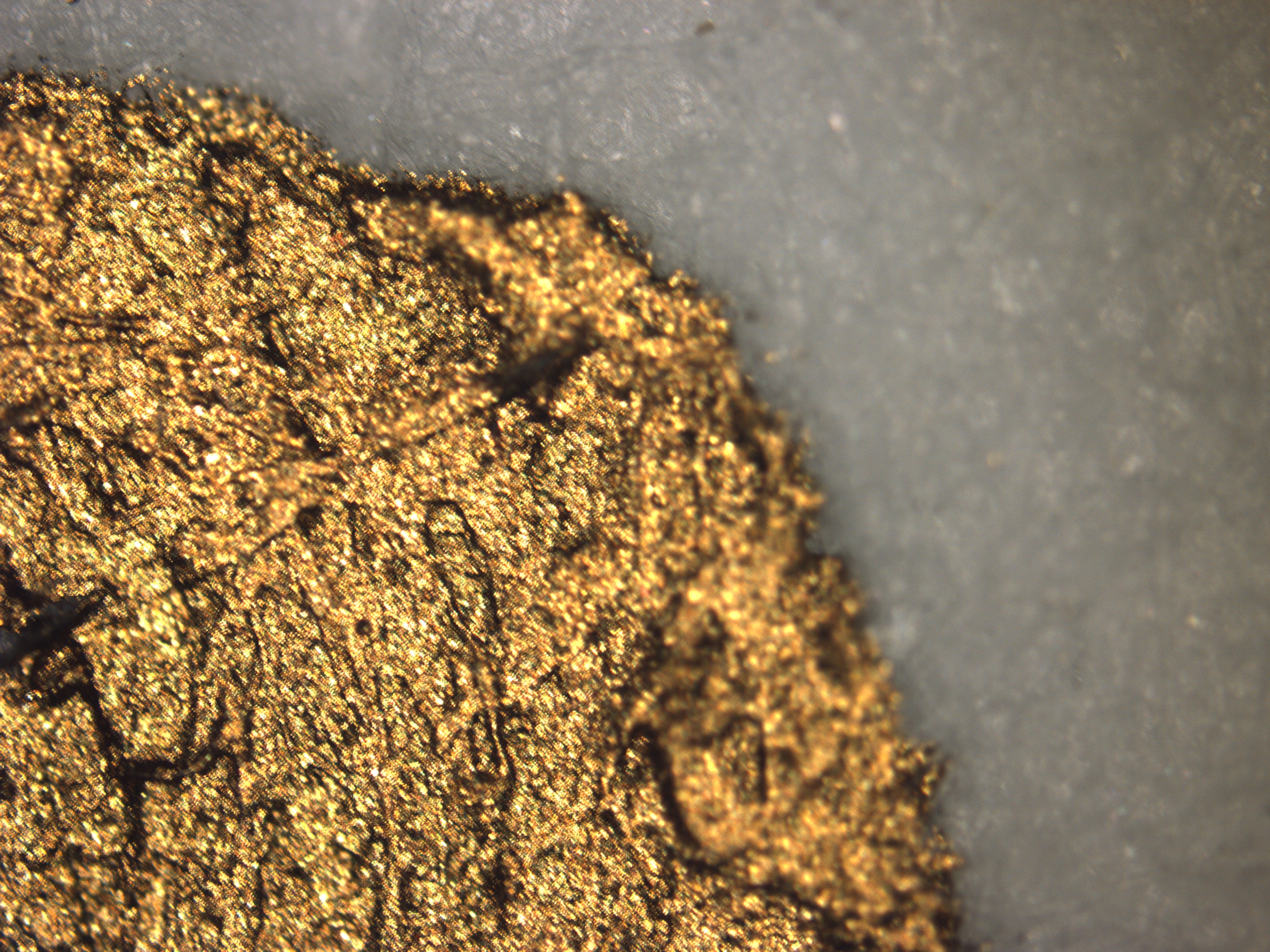
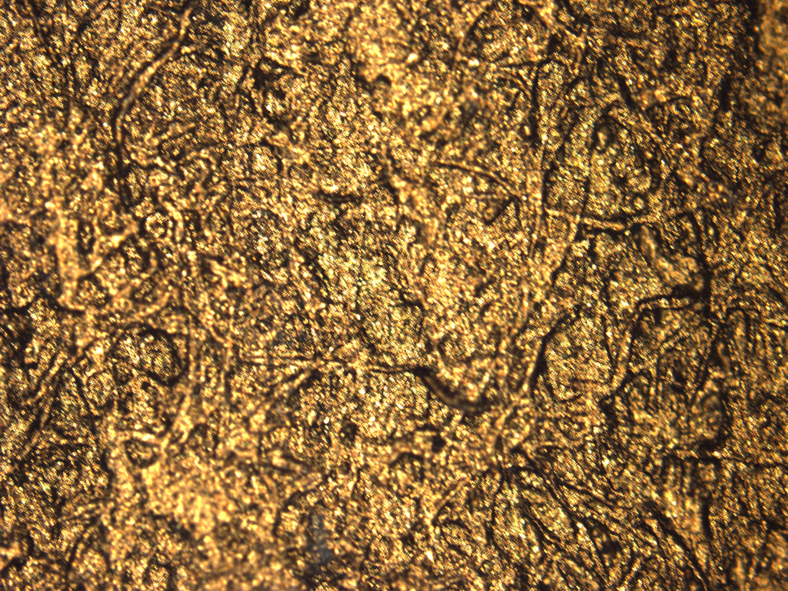
Figure 1 - Bright field light microscopy
images of the gold sharpie with a 10x objective. The left image
shows the edge of the applied ink on the paper while the right image
shows a section in the middle of the sample.
Figure 2 shows the micrographs taken with an SE2 detector of the flaky
structure of the gold sharpie on the course mixed media paper. A clear
boundary between the paper and the sharpie ink is visible. This was
hypothesize to be due to the vastly different composition between the
paper and the ink.
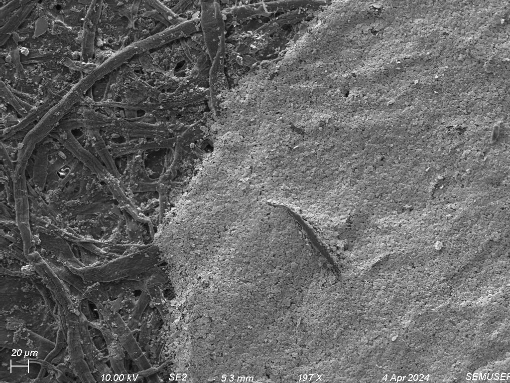
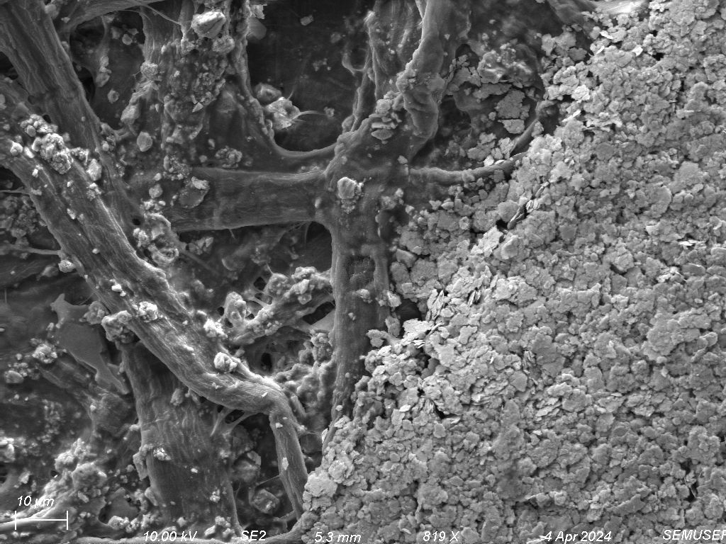
Figure 2 - Secondary electron Micrographs
of the gold sharpie ink on paper at 197x magnification (left) and
819x magnification (right). Both images were taken at a working
distance of 5.3mm and an accelerating voltage of 10kV.
\ This hypothesis is supported by Figure 3, depicting BSD, InLens, and SE2
images all with the same location, working distance, and accelerating
voltage. The BSD image shows a large contrast between the ink and the
paper with the ink being significantly brighter than paper. This indicates
that the ink contains atoms with a much higher Z than the likely organic
composition the paper it is applied to. Additionally, the InLens image
depicts topological contrast of the sample and thus shows much less
contrast between the ink and the paper. The brighter contrast of the ink
compared to the paper is due to the fact that the ink is applied on top of
the paper and therefore is slightly closer to the InLens detector which
sits directly above the sample. Figure 4 shows BSD, InLens, and SE2
images, all in the same location, working distance, and accelerating
voltage, at a greater magnification where the flaky texture of the ink is
more distinguishable. Again, the textured topology of the flakes are
evident through high contrast in the InLens image, whereas the uniformly
bright BSD image shows the homogeneity of the ink.
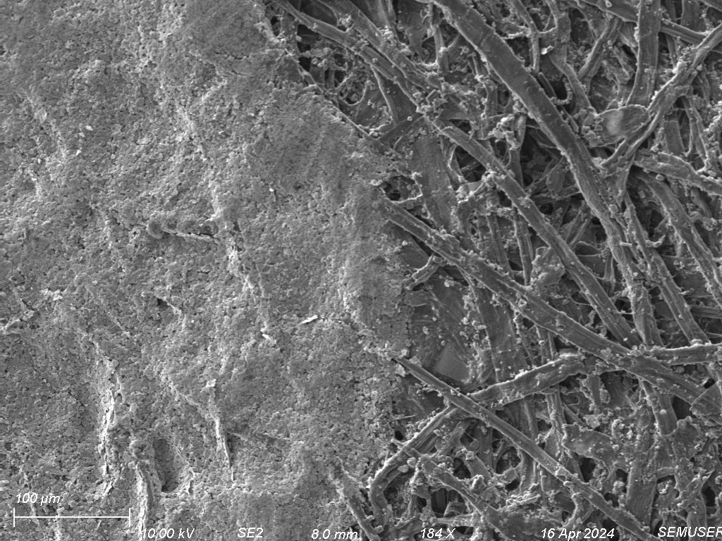
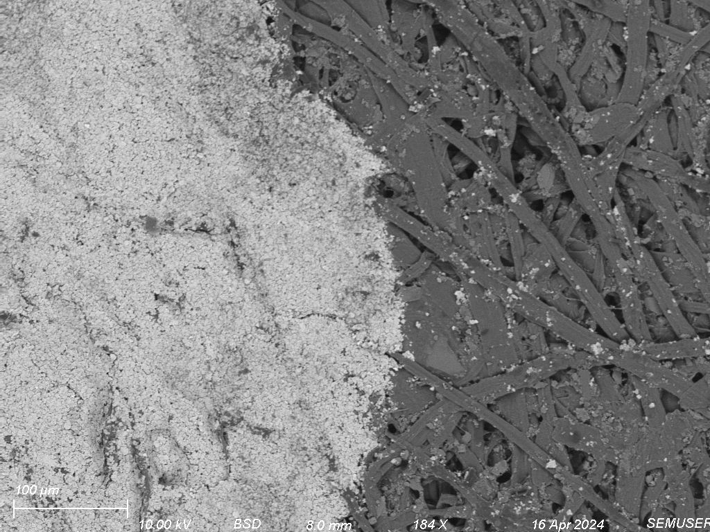
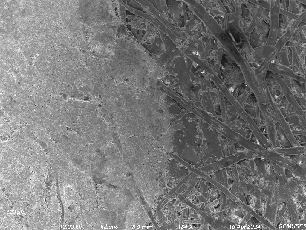
Figure 3 - Micrographs of the gold
sharpie at 184x magnification, a working distance of 8mm, and an
accelerating voltage of 10kV taken with the SE2 detector (left), the
back scattering detector (middle), and the InLens detector (right).
All images were taken in the same position for direct comparison.
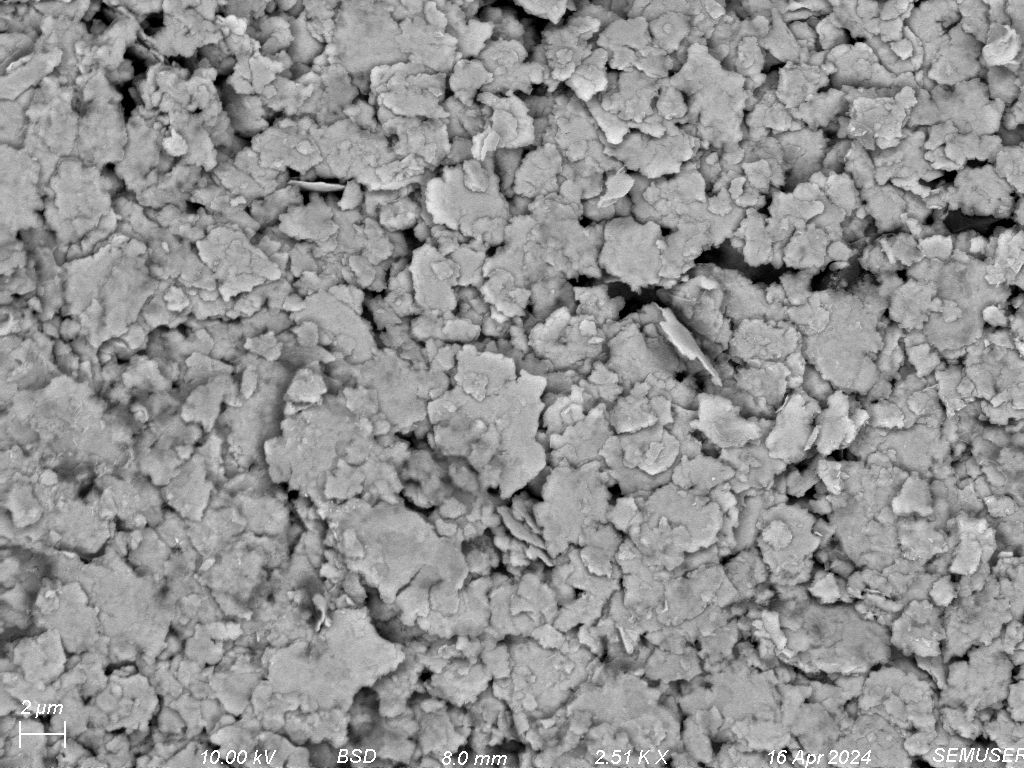
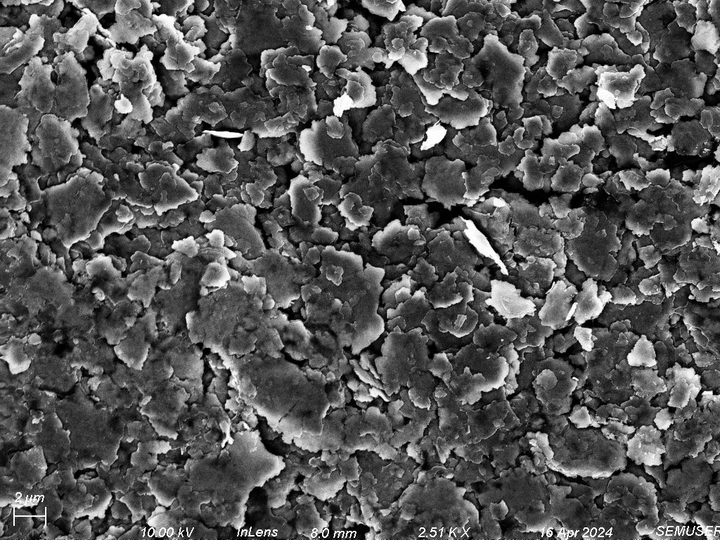
Figure 4 - Micrographs of the gold
sharpie at 2.51kx magnification, a working distance of 8mm, and an
accelerating voltage of 10kV taken with the SE2 detector (left), the
back scattering detector (middle), and the InLens detector (right).
All images were taken in the same position for direct comparison.
The elemental composition of the gold sharpie was investigated via EDS. It
should be noted that not all the elements identified by the software were
included in the spectra or the elemental composition used for mapping. Due
to EDS’s low spectral resolution, it is common for errors to be made in
labeling elements. Thus, it is vital to use the knowledge of the sample to
determine whether an element is likely to exist in the sample. For
example, due to Vanadium’s rarity, it is not likely to exist in the gold
sharpie ink despite being identified by the software as in the spectra.
Thus, it was not included in either the reported spectra or the the
elemental mapping. Figure 5 contains the spectra obtained by EDS analysis
and it is clear that the gold sharpie contains copper, likely giving the
sharpie it's gold appearance. Additionally, organic elements, such as
carbon and oxygen, appeared on the spectra as well, likely mainly
originating from the paper. In order to get a clear idea as to which
elements were comprised in the ink and which were comprised in the paper,
elemental mapping was performed. Figure 6 clearly shows that the copper x
ray signal comes from the ink, while the majority of the carbon and oxygen
signal come from the paper. Additionally, a significant amount of x ray
signals attributed to calcium were mainly located on the paper rather than
in the ink, while significant amounts of sodium appeared in the ink. This
leads to the conclusion that the gold sharpie is mainly composed of a
copper salt.
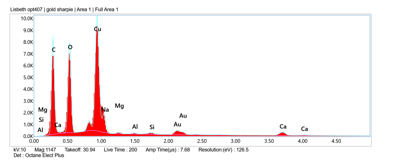
Figure 5 - ESD spectrum of the gold
sharpie ink on paper taken at an accelerating voltage of 10kV and a
working distance of 5mm.
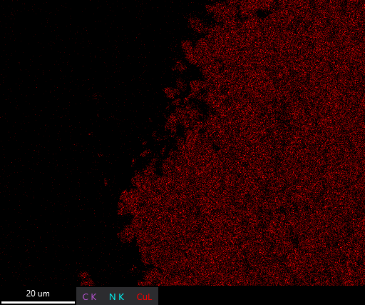
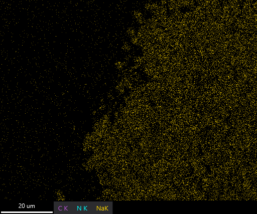
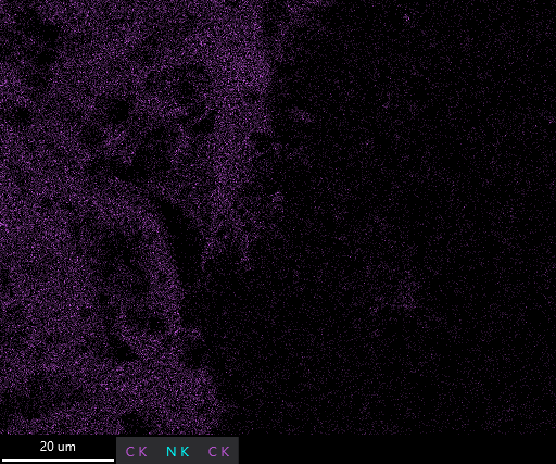
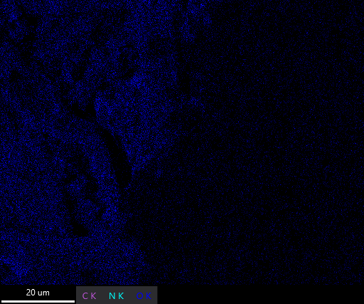
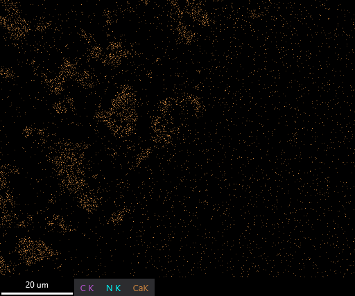
Figure 6 - EDS mapping images of the gold
sharpie ink on paper taken at an accelerating voltage of 10kV and a
working distance of 5mm. From left to right: SE2 field of view
image, copper elemental EDS mapping image, sodium elemental EDS
mapping image, carbon elemental EDS mapping image, oxygen elemental
EDS mapping image, calcium elemental EDS mapping image.
3.2 Gel Pen
Bright field images on the light microscope at 10x magnification were taken at the edge of the applied gel pen ink with the paper in view, and in the middle of the sample and depicted in Figure 7. This demonstrates the true color of the gel pen as well as the ink's nonuniform coverage on the paper.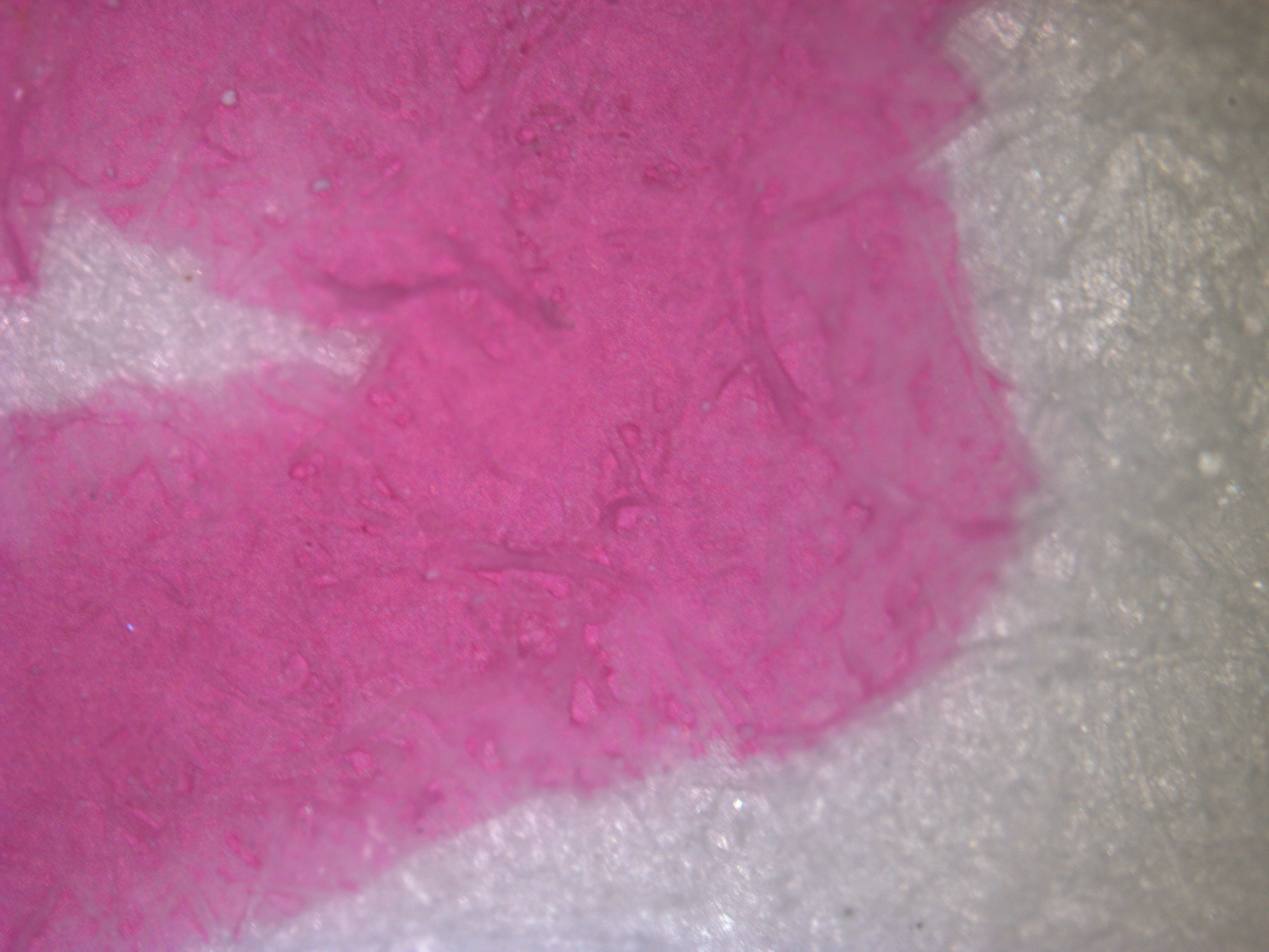
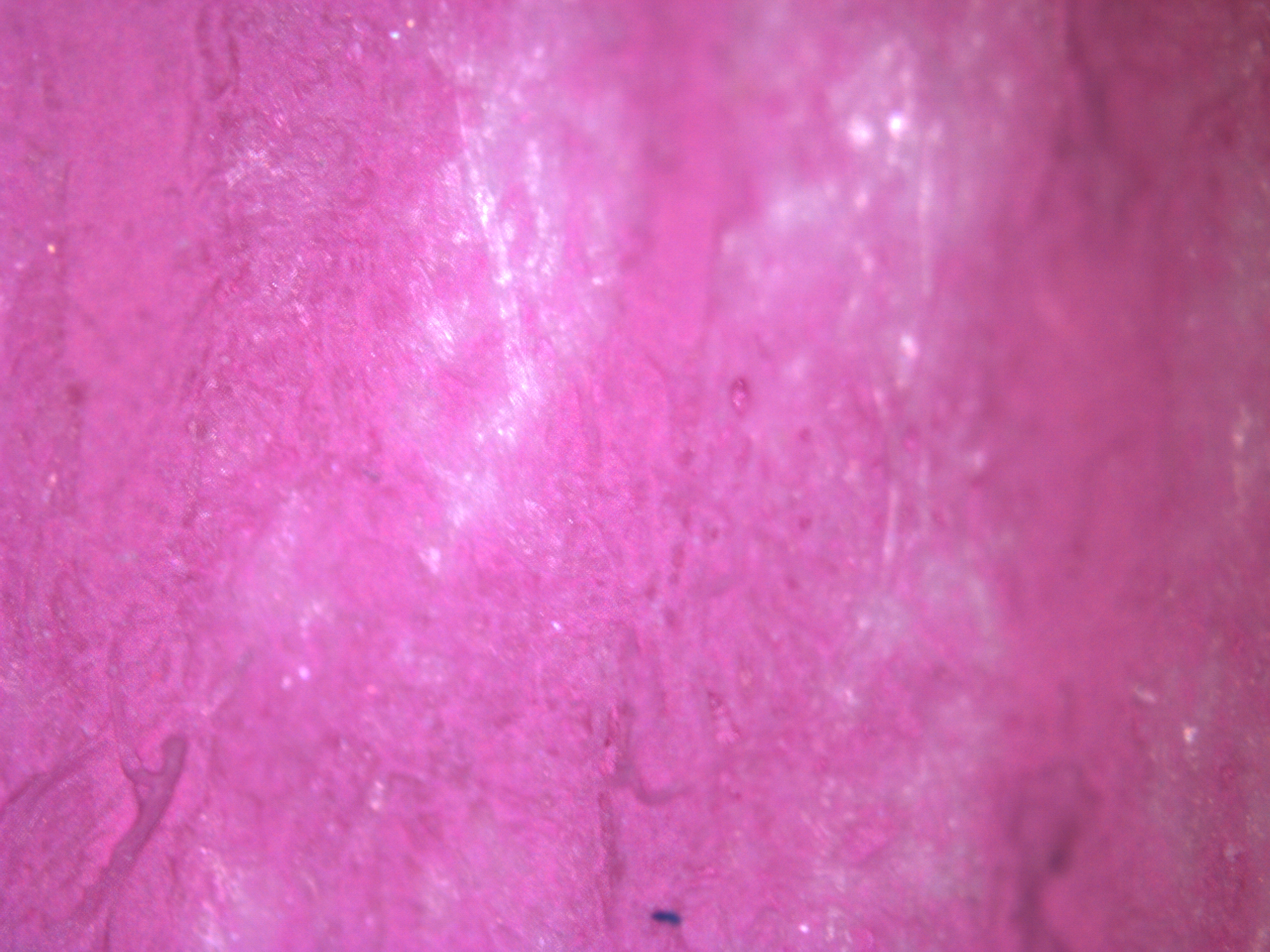
Figure 7 - Bright field light microscopy
images of the gel pen with a 10x objective. The left image shows the
edge of the applied ink on the paper while the right image shows a
section in the middle of the sample.
Figure 8 shows SE2 micrographs of the gel pen and two different spheres
are clearly visible contained in the ink. The inconsistent coverage of
these spheres compared to the gold sharpie aligns with the observation
made in the light microscope images that the gel pen isn't uniformly
covering the paper.
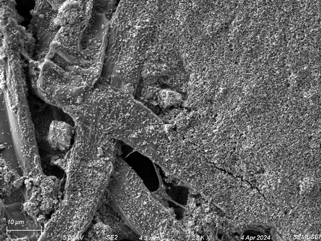
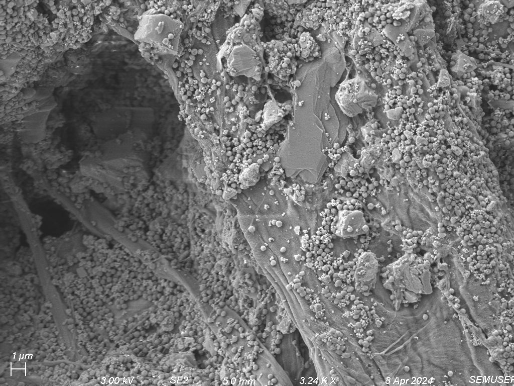
Figure 8 - Secondary electron Micrographs
of the gel pen ink on paper at 1.23kx magnification, working
distance of 4.3mm, and an accelerating voltage of 5kV (left) and t
3.25kx magnification, working distance of 5.0mm, and an accelerating
voltage of 3kV (right).
Further investigation of the spheres' composition was performed on a close
up of an aggregate using various detectors in the SEM. Figure 9 depicts
BSD, InLens, and SE2 images all with the same location, working distance,
and accelerating voltage. The contrast visible in the BSD image shows that
the two different spheres are composed of different materials. The more
even contrast in the InLens image show how the spheres lay on top of each
other compactly. EDS analysis was performed but did not provide any
conclusive information about the composition of the of the spheres. This
is likely due to a few factors. First, the spheres are relatively small,
with the large spheres between 200-300nm. This makes it hard for the EDS
spatial mapping to resolve the of the composition of the spheres due to
the large interaction volume of the beam, especially within the compact
aggregates. Additionally, because the accelerating voltage is set at 10kV,
not all atoms are able to be detected in the spectra, so it's possible
that some elements that exist within sample are not detected by the EDS.
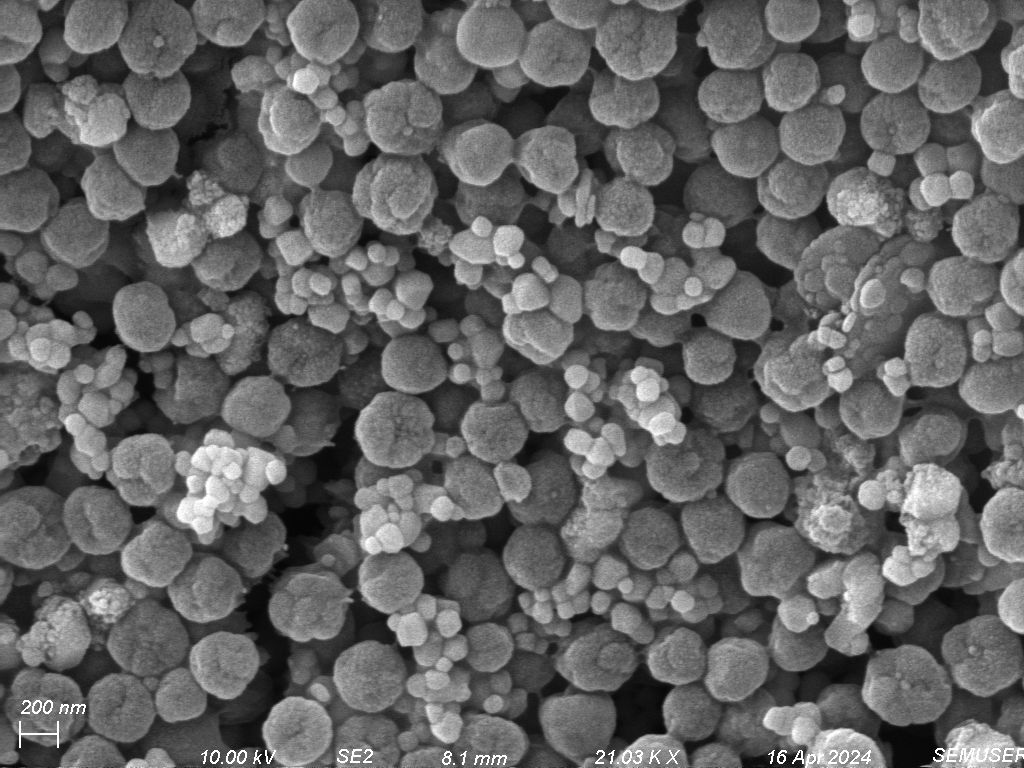
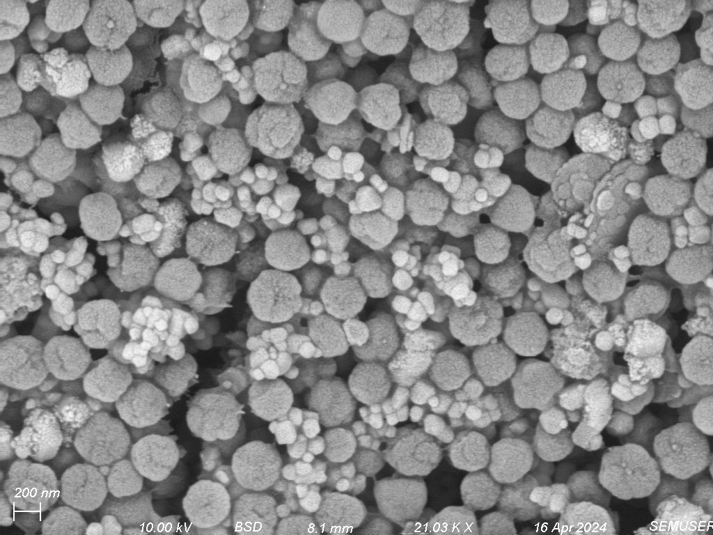
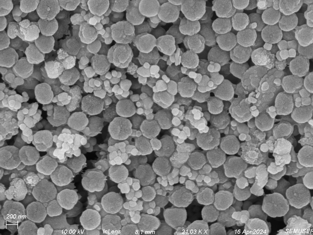
Figure 9 - Micrographs of the gel pen at
21.03kx magnification, a working distance of 8.1mm, and an
accelerating voltage of 10kV taken with the SE2 detector (left), the
back scattering detector (middle), and the InLens detector (right).
All images were taken in the same position for direct comparison.
3.3 Acrylic Paints
Figure 10 shows bright field images on the light microscope at 10x magnification taken at the edge of each of the applied acrylic paints with the paper in view, as well as in the middle each of the samples. Each paint is slightly transparent and the paper is visible through the paint, but the coverage appears uniform. Additionally, the true color for each paint is visible in these images.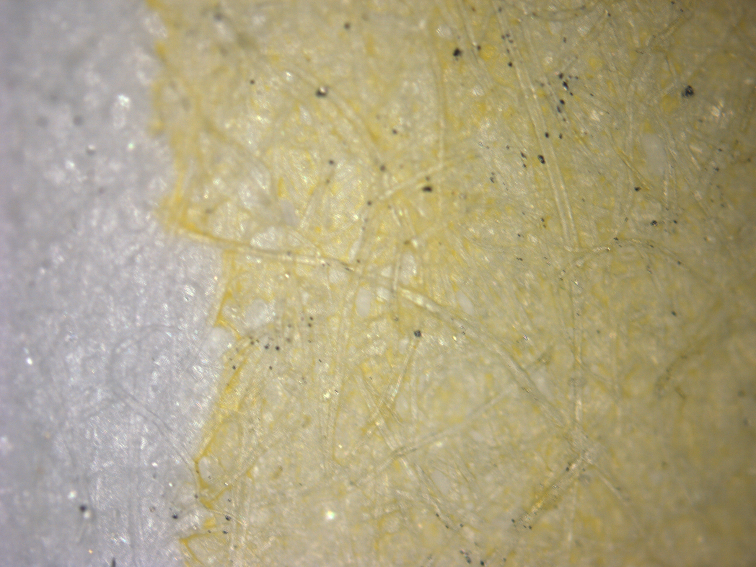
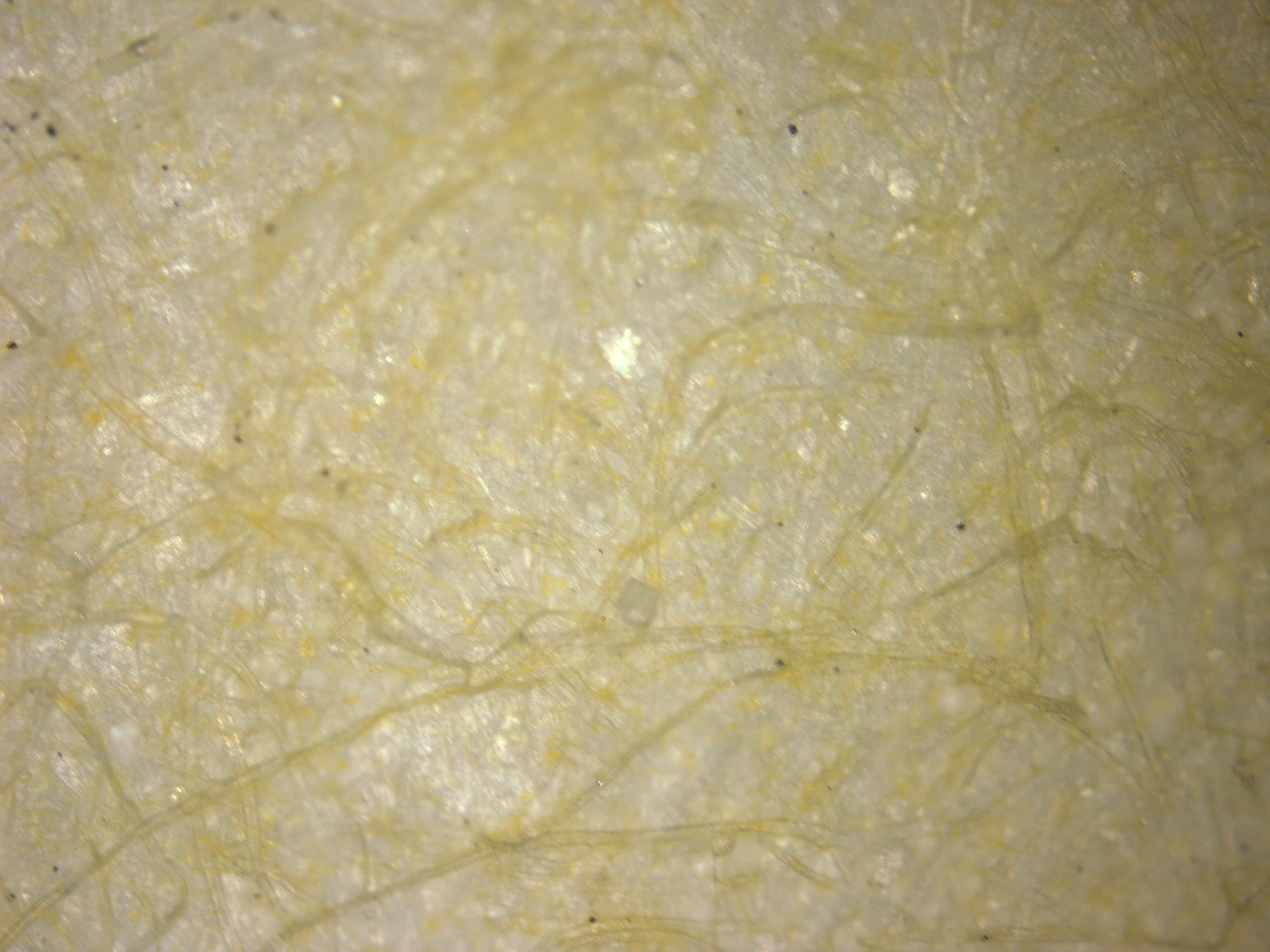
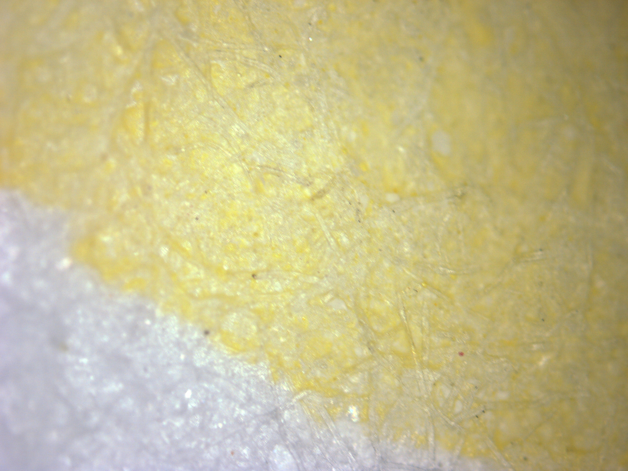
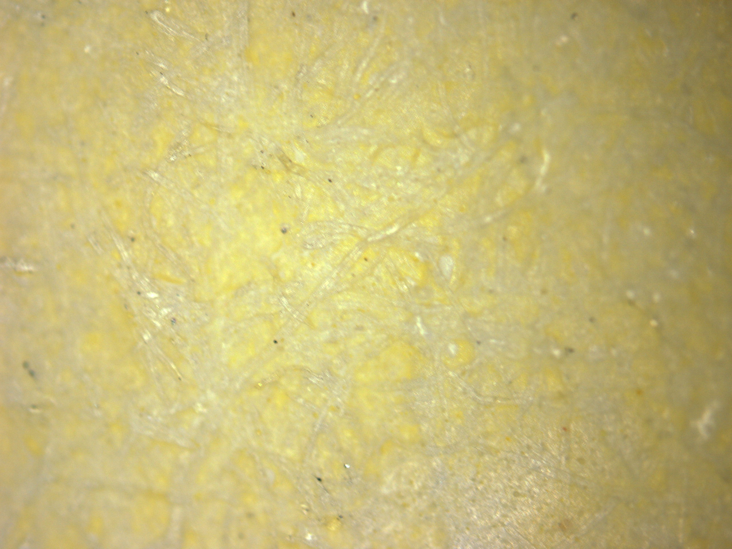
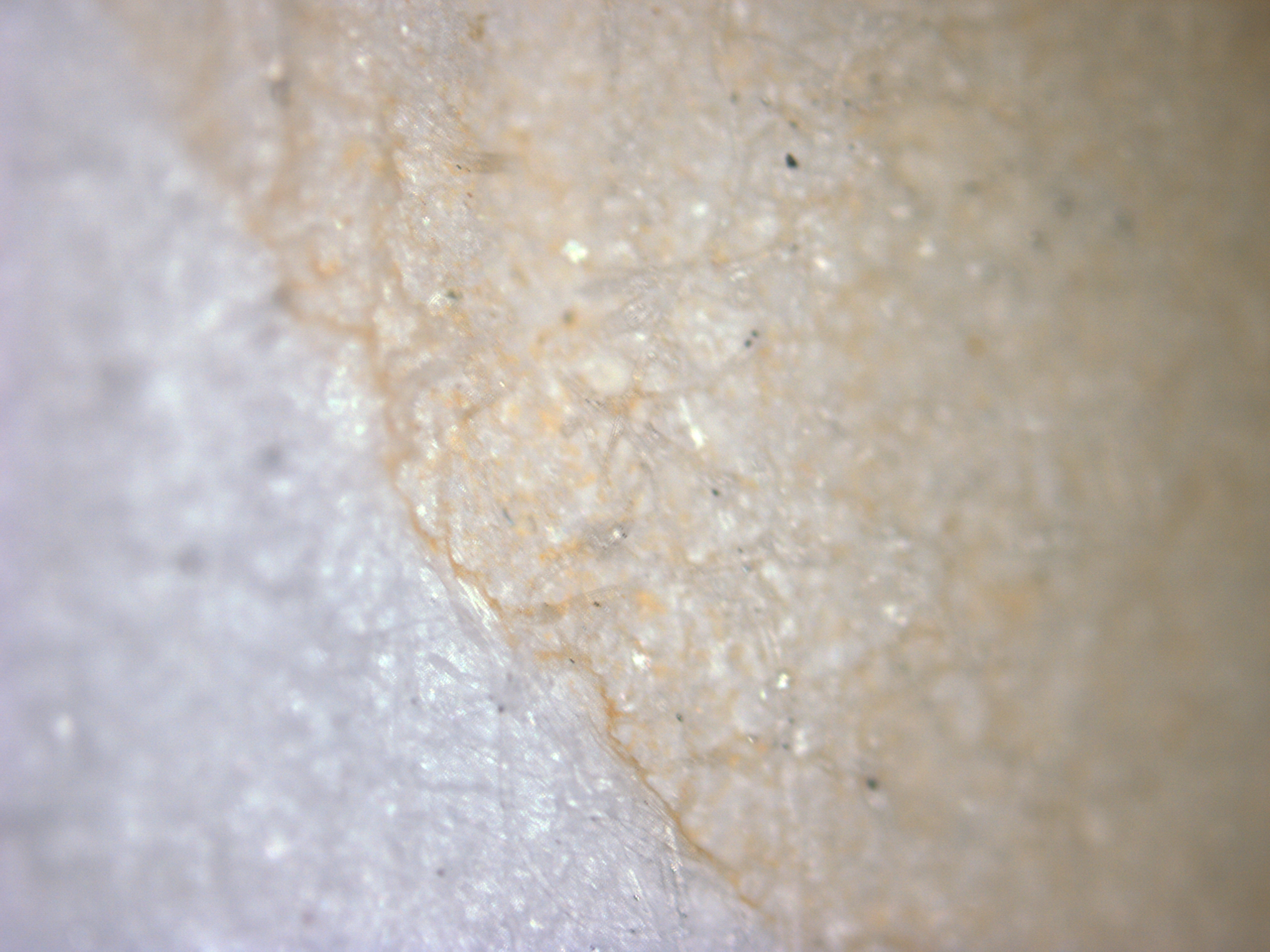
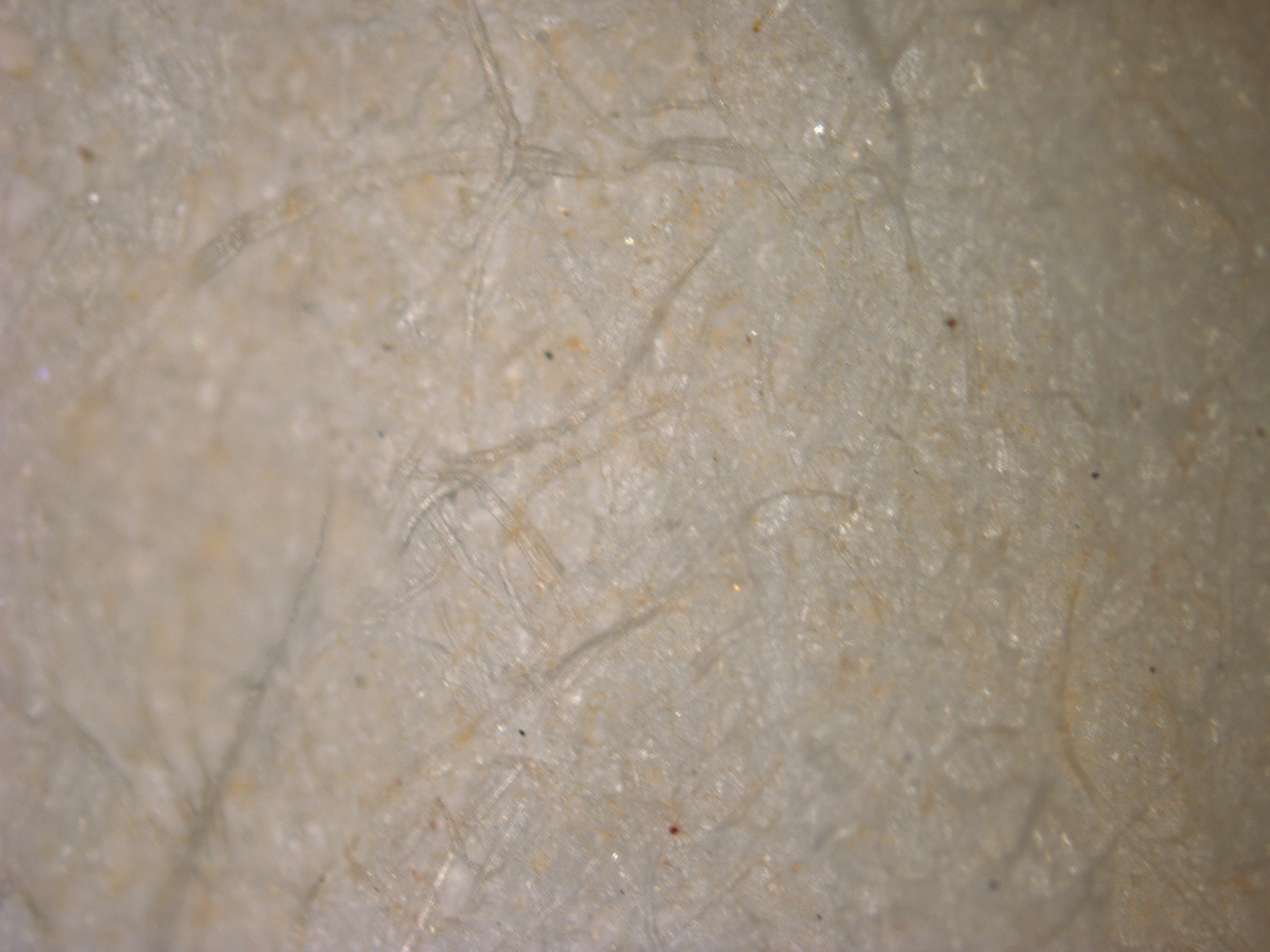
Figure 10 - Bright field light microscopy
images of the three acrylic paints with a 10x objective. From left
to right: best quality paint at the edge of the applied paint on
paper, best quality paint in the center of the sample, next best
quality paint at the edge of the applied paint on paper, next best
quality paint in the center of the sample, lowest quality paint at
the edge of the applied paint on paper, lowest quality paint in the
center of the sample.
Figure 11 shows SE2 micrographs of each of the various quality acrylic
paints. None of the paints had as neat of a microstructure as either of
the ink, however differences between the different paints is apparent. The
two lowest quality paints are the "messier" than the high quality paint,
with the smaller and more irregular shaped particulates. The highest
quality paint had fewer small particulates, giving a "cleaner" look.
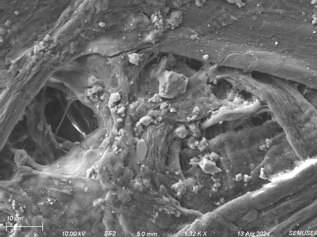
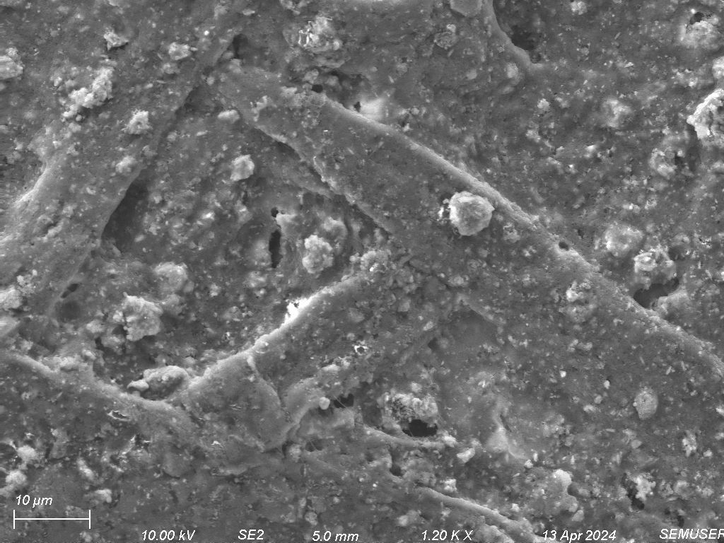
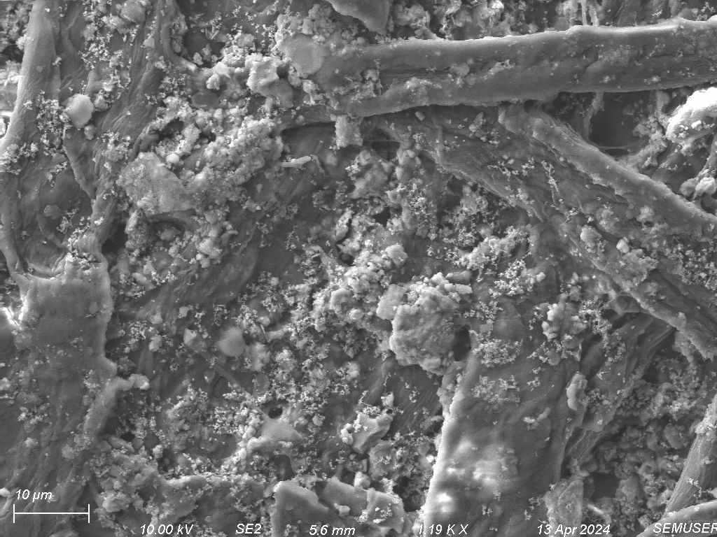
Figure 11 - Secondary electron
Micrographs of the gel each of thr acrylic paints taken at an
accelerating voltage of 10kV on paper. From left to right: the
highest quality paint at 1.32kx magnification and a working distance
of 5mm, the next highest quality paint at 1.20kx magnification and a
working distance of 5.0mm, and the lowest quality paint at 1.19kx
magnification and a working distance of 5.6mm.
EDS analysis was performed an all the paint samples. The spectra showed
Oxygen, Carbon, and Calcium were all shown to be present in all three of
the EDS spectra, however they were not included in this this figure since
most of the signal was determined to comes from the paper, consistent with
the conclusions drawn from the elemental mapping of the gold sharpie. An
EDS mapping analysis of the lowest quality paint is shown in Figure 12.
The main components found in the paint were silicon, aluminum, Titanium,
and Magnesium. Figure 13 shows EDS mapping of the next lowest quality
paint, containing silicon, aluminum and magnesium. Figure 14 shows the
highest quality of paint and showed the fewest elements, with only
magnesium and silicon being distinguishable. It is interesting to note
that with increasing quality of paint, fewer elements were identified.
These conclusions however should be met with skepticism however, for
reasons outlined in the previous EDS discussions.
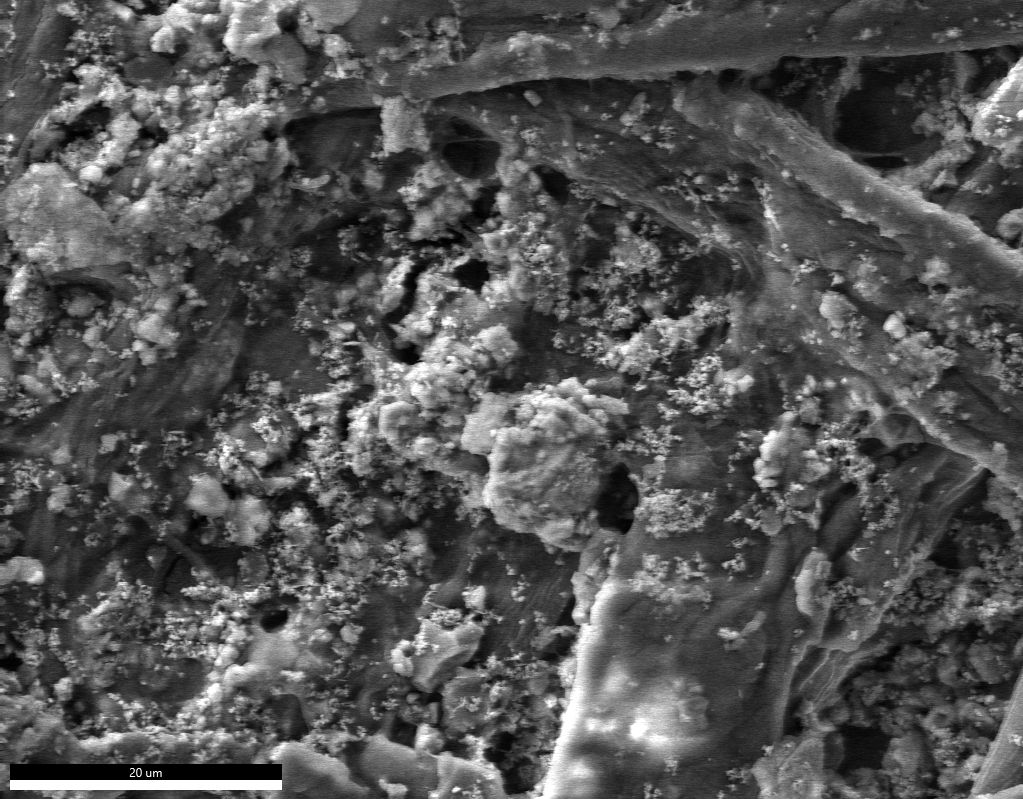
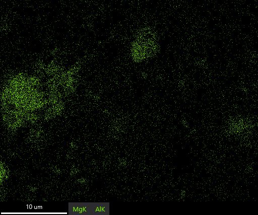
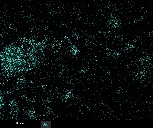
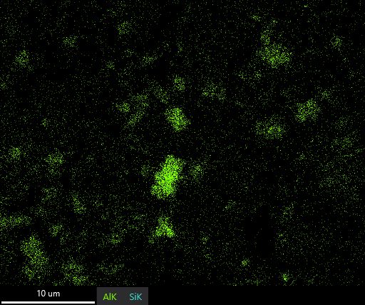
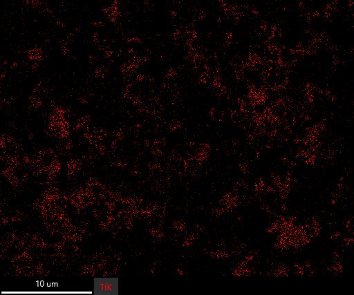
Figure 12 - EDS mapping images of the 2nd
lowest quality acrylic paint on paper taken at an accelerating
voltage of 10kV and a working distance of 5mm. From left to right:
SE2 field of view image, Mg elemental EDS mapping image, Si
elemental EDS mapping image, Al elemental EDS mapping image, and Ti
elemental EDS mapping image.
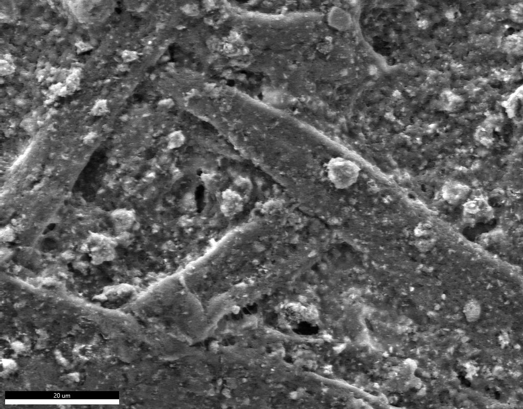
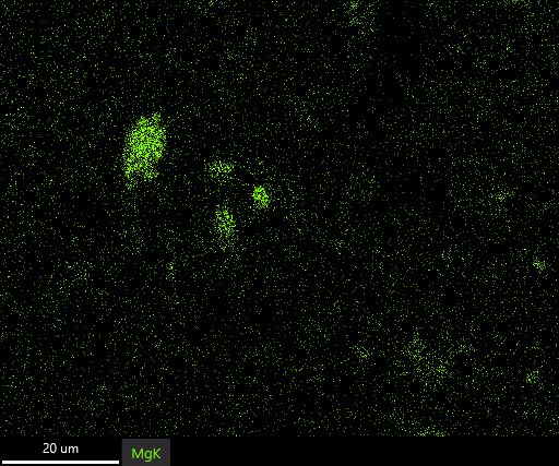
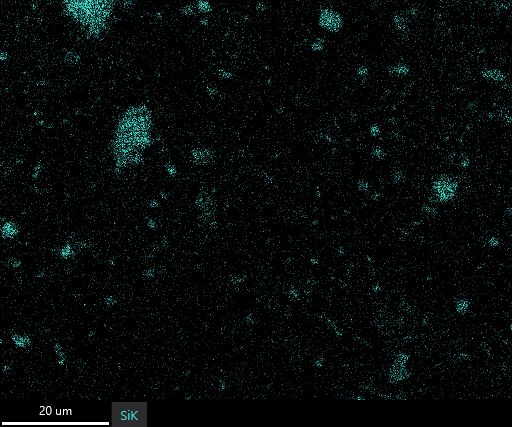
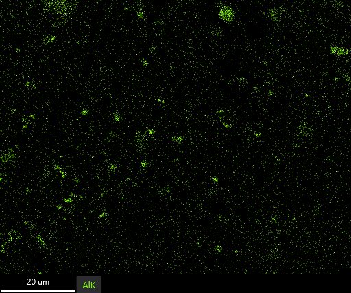
Figure 13 - EDS mapping images of the 2nd
lowest quality acrylic paint on paper taken at an accelerating
voltage of 10kV and a working distance of 5mm. From left to right:
SE2 field of view image, Mg elemental EDS mapping image, Si
elemental EDS mapping image, and Al elemental EDS mapping image.
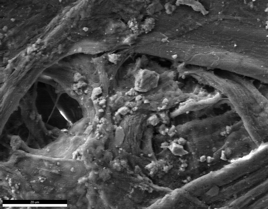
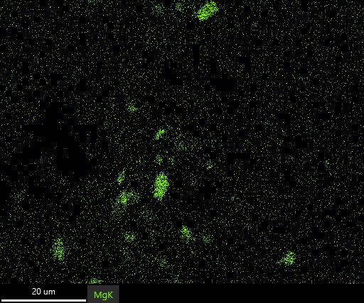
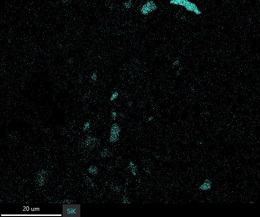
Figure 14 - EDS mapping images of the
highest quality acrylic paint on paper taken at an accelerating
voltage of 10kV and a working distance of 5mm. From left to right:
SE2 field of view image, Mg elemental EDS mapping image, and Si
elemental EDS mapping image.
4. Conclusion
If you're like me, hopefully the next time you pull out your gold sharpie to mark off the end of the day on your calendar, or your gel pens to write out a thank you letter to a loved one, or your set of acrylic paints to express your creativity, you can appreciate the interesting and beautiful microscopic structure hidden within your artistic expression. :)
Acknowledgments
Thank you to Sean and Gregg for their support in this project, especially Sean, for helping me struggle through the EDS software.