Lokendra Singh Dhami
PhD Student
Department of Physics and Astronomy, University of Rochester
ldhami@ur.rochester.edu
1. Introduction
Silicon quantum dots are promising candidates for spin-based quantum computation. They consist of Si/SiGe substrate on top of which is an electrically insulating oxide (SiO2) layer. A multilayer gates lies above the oxide layer which is fabricated by using electron beam lithography (EBL) and metal deposition. The arrangement of different layers of Al gates when tuned by suitable electrical potential confines electron which must be kept isolated (at cryogenic temperatures) for any spin based quantum computation.
Owing to only few hundreds of nanometer size, the characterization of silicon quantum dots requires used of electron microscopy (EM) techniques. In this project work, we have used different EM techniques learned in OPT 307/407 to characterize the quantum dots. Our feature of interest are the Aluminium (Al) gates which are only tens of nanometer thick and require suitable imaging conditions for their optimal viewing. On top of this, we used Focused Ion Beam (FIB) to reveal the cross-section of Al gates.
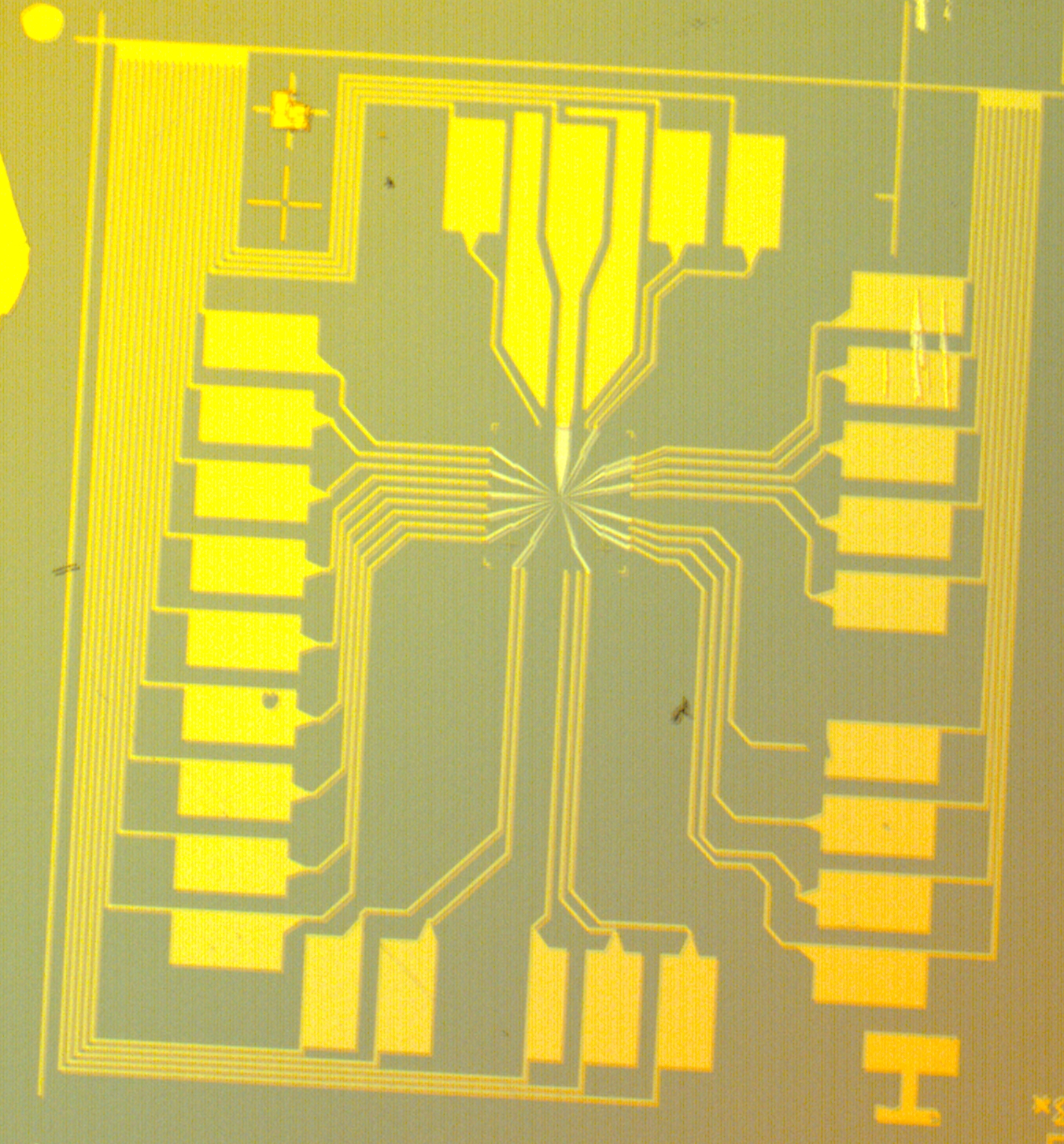
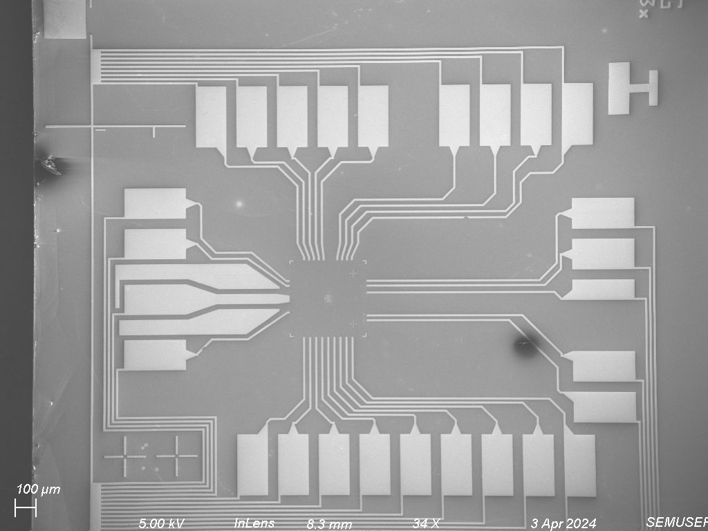
2. Characterization Using EM TechniquesThe quantum dot used for this study was a part of 2 * 2 array of quantum dots in a 6 * 6 mm Silicon (Si) chip. In Figure 1, we see a Light Microscope (LM) image of a quantum dot at 5x magnification. Most of what is visible in Figure 1 are bond pads that provide a means to connect quantum dot at the center to external circuitry for proper voltage biasing which is essential for trapping an electron.
To get a closer look at the center, we can increase the magnification of LM and the images obtained for 10x and 100x magnifications are shown in Figure 2.
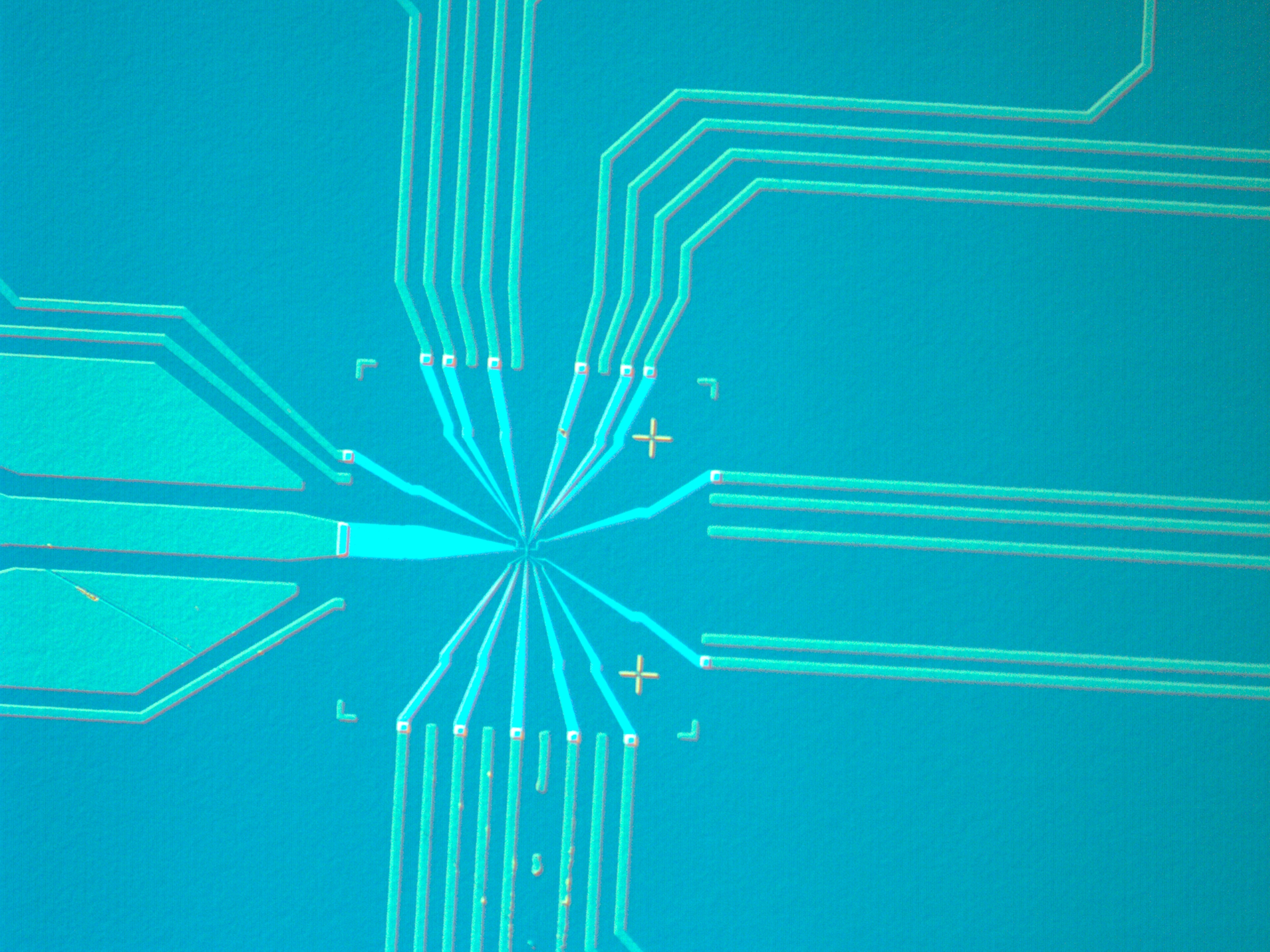

We can see the gate architecture in Figure 2 but a higher magnification is desired. At 10x magnification, we can see the connection between bond pads and Aluminium (Al) gates clearly. At 100x magnification we can get a better look at the gates themselves but not at the region where electrons are trapped. Our feature of interest at this point is the center of of 100x image in Figure 2 (right). This is not possible with LM. Hence we resort to scanning electron microscopy techniques in the next section.
A. Scanning Electron Microscopy (SEM)The Si chips used in this study had 80 mm thick Gold (Au) layer deposited during their fabrication for easy viewing in SEM. The Au layer improves the resolution since its higher Z value reduces the interaction volume of electron beam. Since the feature we are looking at is only few nanometers, the challenge was to find optimal viewing conditions. Hence, we tried different accelerating voltage, working distance, and detector to find the optimal viewing conditions.
When we viewed our sample at 20 kV accelerating voltage under SE2 detector the images we found are shown in Figure 3.
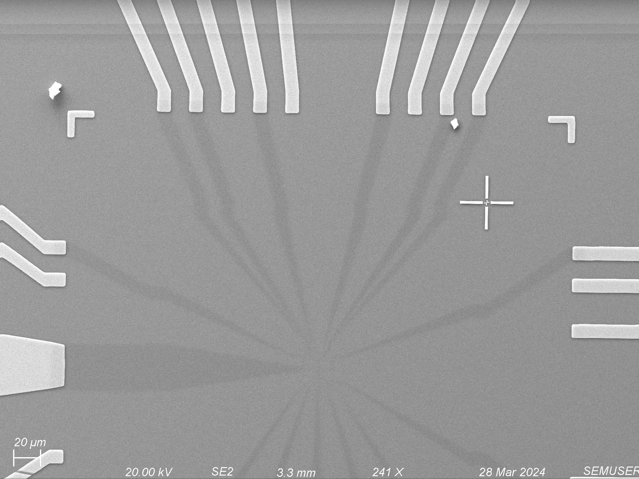
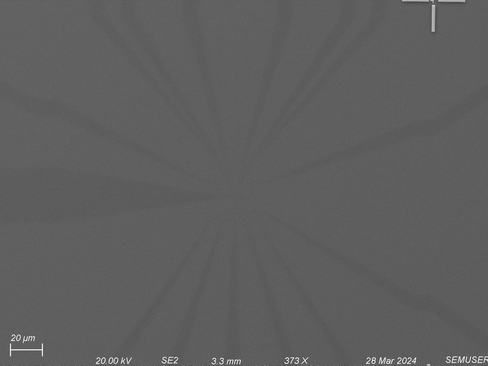
In Figure 3 (left), we see the image of Al gates in connection with bond pads at 241x magnification but the gates are seen only as shadows. When we tried to increase the magnification to 373x (right), no improvement is seen.
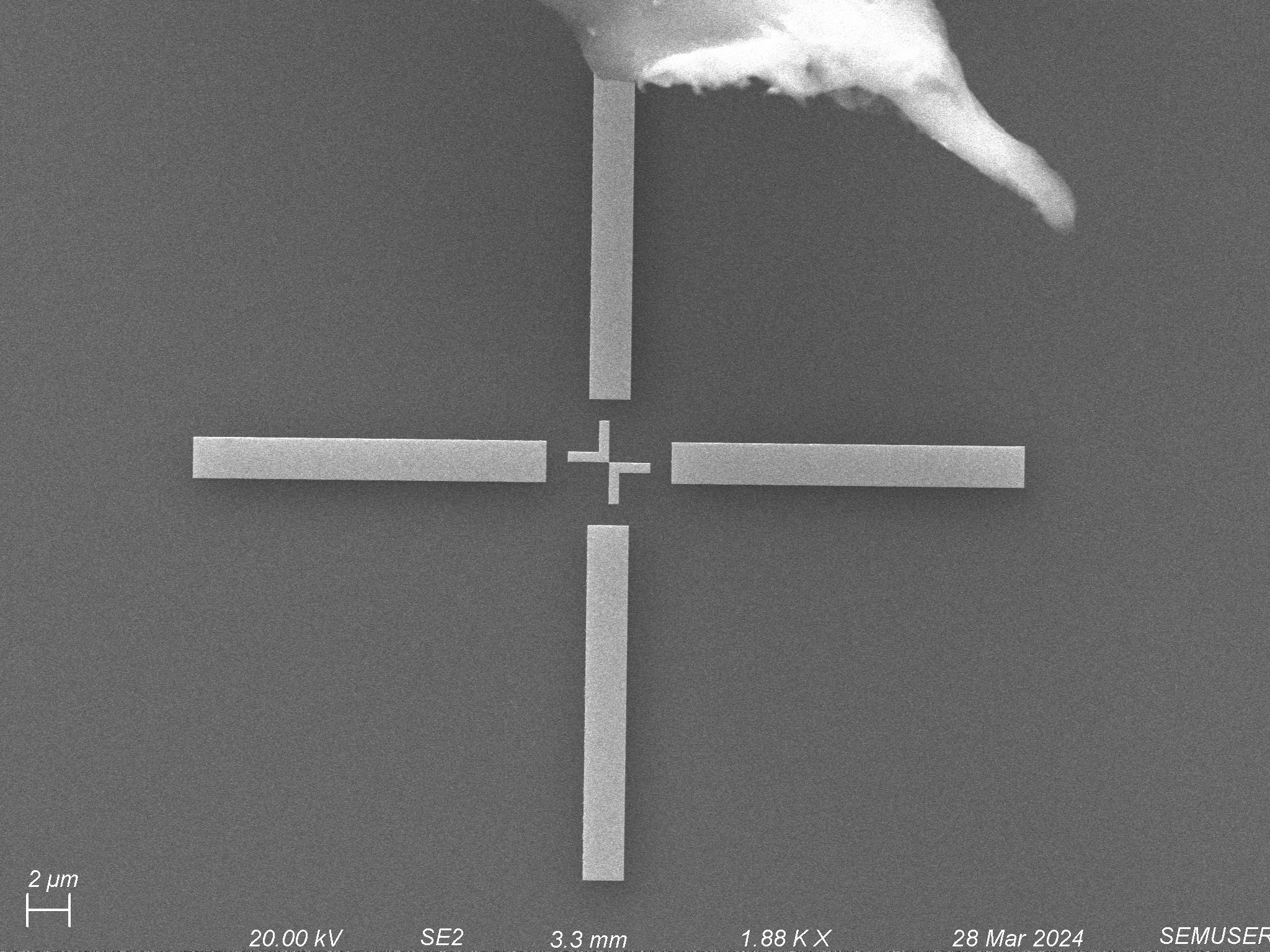
To make sure that this is not the problem with focus and/or brightness/contrast, we imaged a chip alignment mark (Figure 4). Even with higher magnification (1.88kx), the alignment mark was imaged nicely. The cloud-like matter at the upper edge of the mark is due to contamination of the sample. This means our imaging conditions are not ideal for the feature we want to look at.
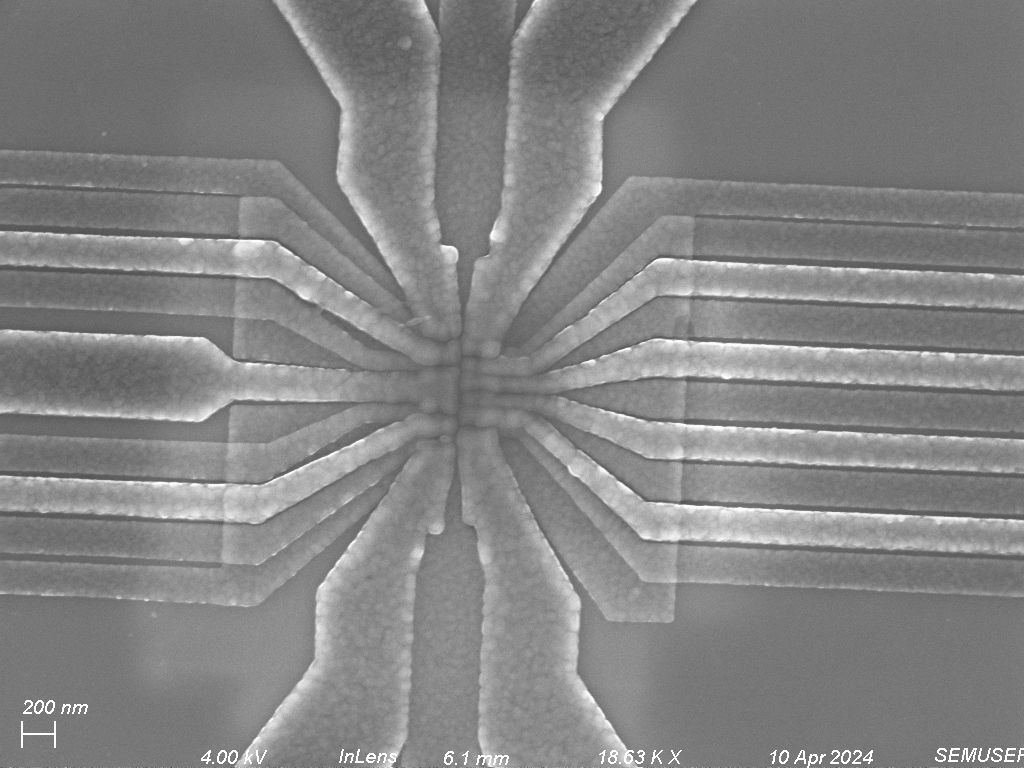
Next, we tried to switch the detector to InLens which provides better imaging of topography of sample. We also lowered the working voltage to 5 kV. The images obtained are shown in Figure 5.
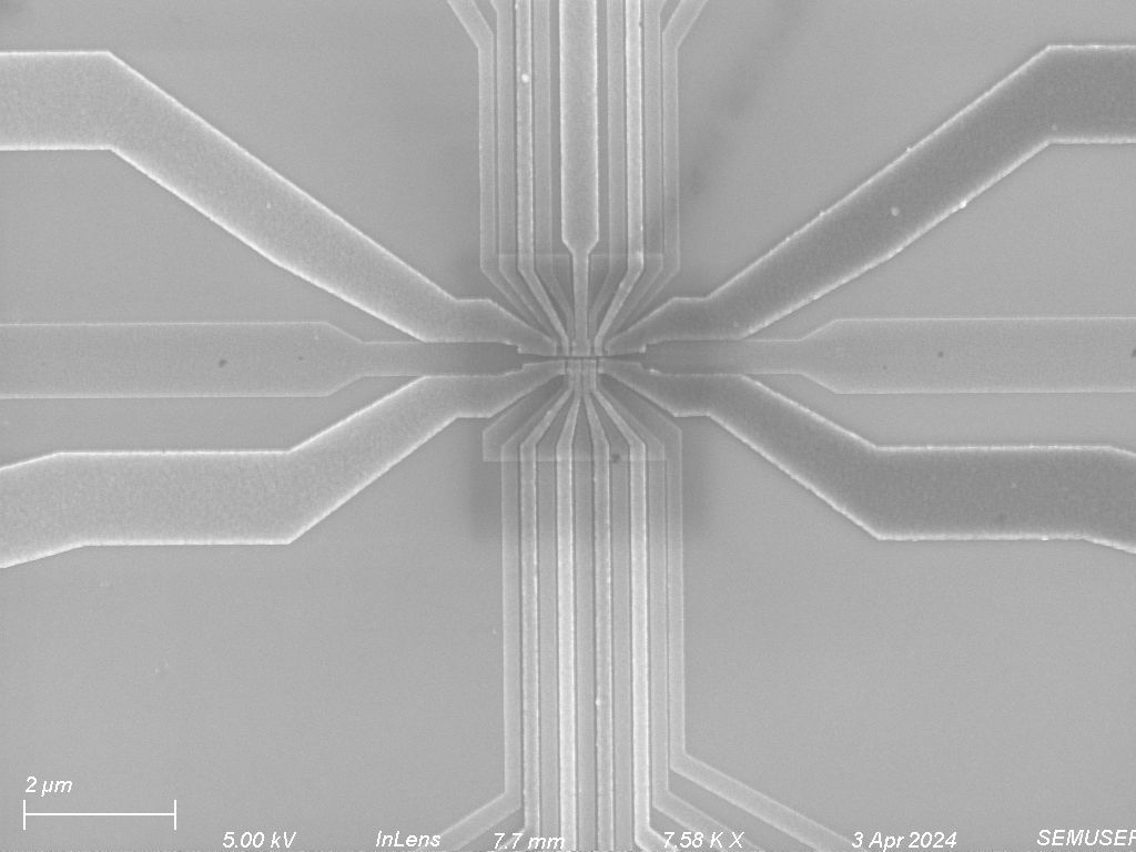
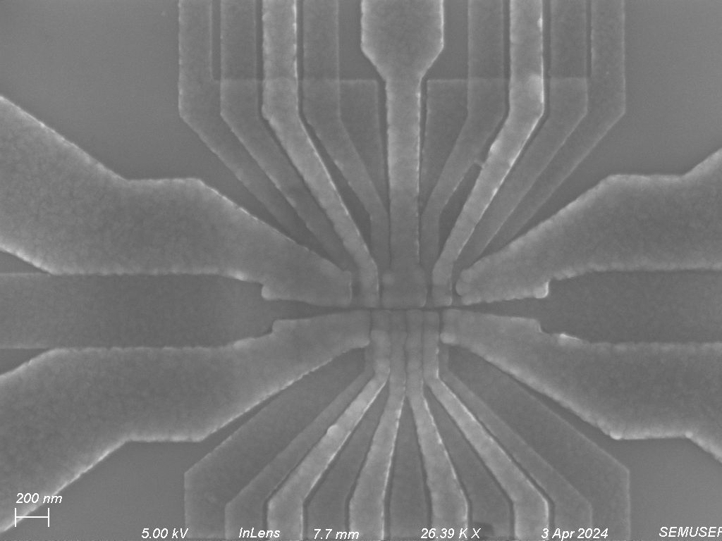
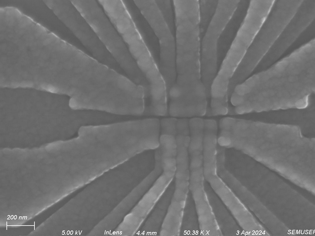
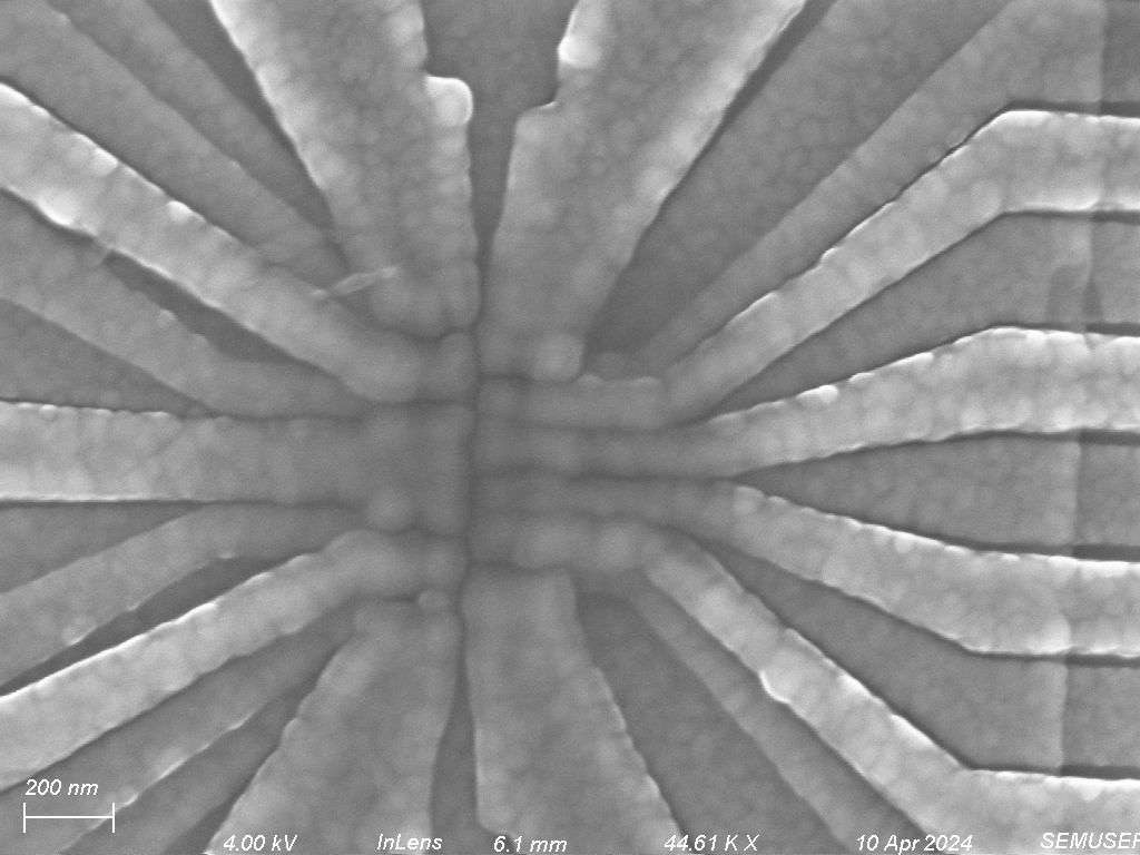
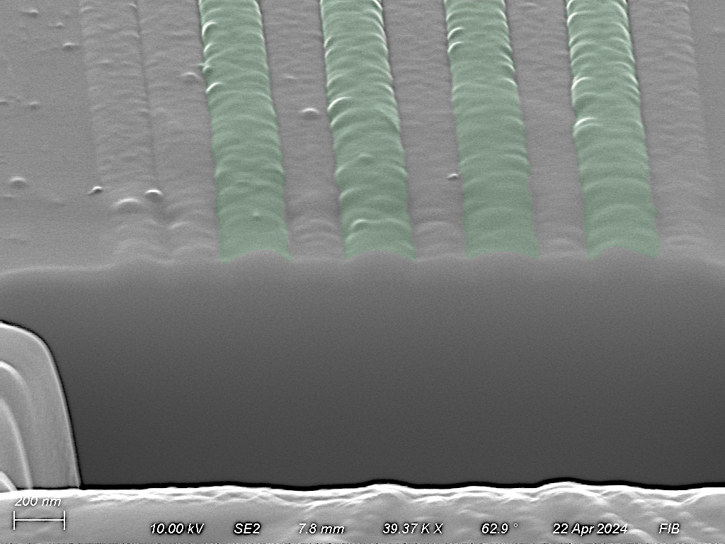
In Figure 7 we see the corresponding images of Figure 6 at 4 kV. The images now have better brightness/contrast and focus. Also, the topography of the Al gates is now more visible confirmed by the better view of the grainy nature of Al gates.
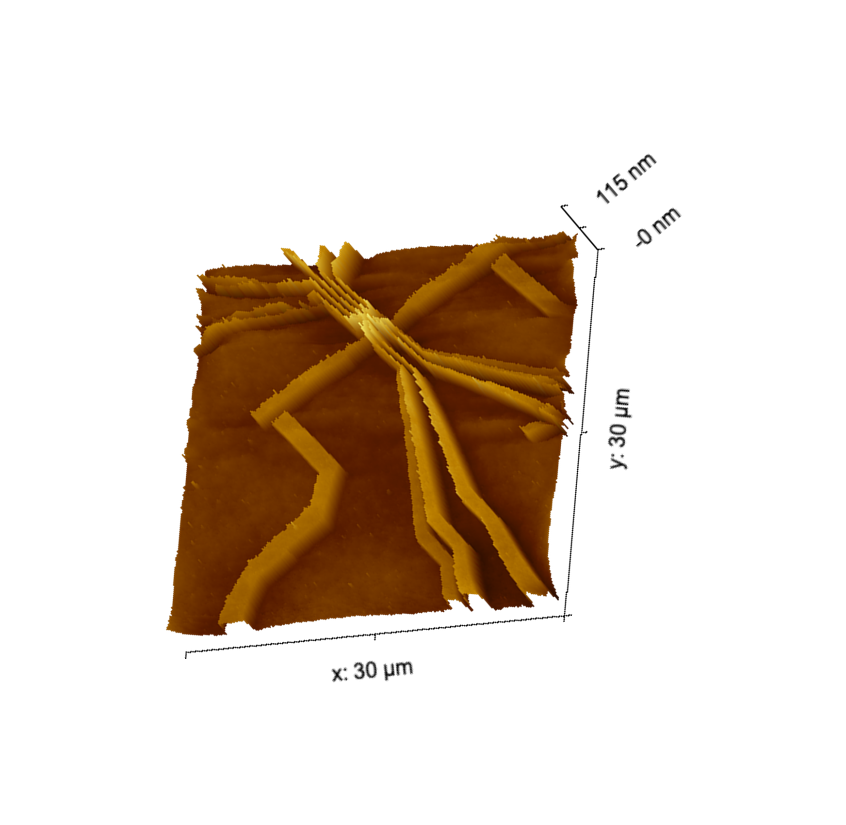
B. Atomic Force Microscopy (AFM)We performed AFM imaging to generate a height profile and hence the 3D image of the gate architecture. For this purpose we used semi-contact mode of AFM. We see that the gates are somewhere near hundred nanometers thick.
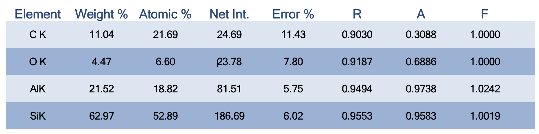
We performed X-ray microanalysis using EDS to confirm the existence of elements that we expect to be present. The chip has Si/SiGe substrate on top of which is a Silicon dioxide (SiO2) layer. This is followed by four layers of Al gates. Since Au and Cr were also deposited during the fabrication of the chip for improving imaging conditions, we expect them to be present in the EDS analysis.
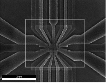
The region shown by a square in Figure 9 (left) was used for the EDS analysis with drift-correction turned on. We used lower (10 kV) accelerating voltage since higher voltage may destruct the gates architecture, our primary interest. The Figure (right) shows the relative composition of elements found in the sample in the form of a pie chart.

The quantitative results of EDS analysis are shown in Figure 10. We detected Si, Al, O as expected. The presence of carbon is due to sample contamination (Figure 4). Clearly, the detection of Au and Cr was not possible because of their trace quantities and lower accelerating voltage used as well as the fact that their presence is limited to the lower layers of the chip.
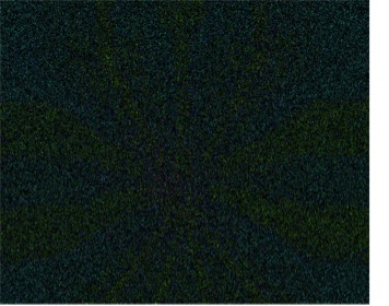
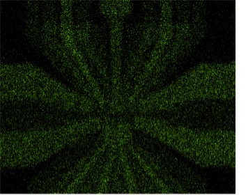
In Figure 12, we see the color map of Al (left) and Si (right).
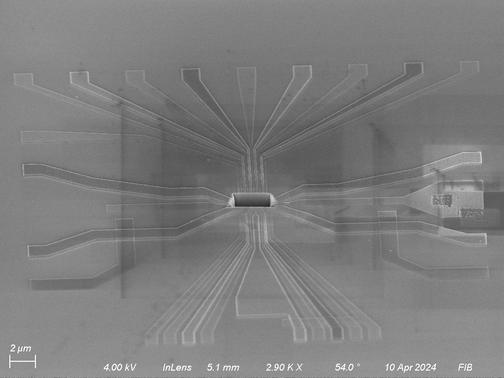
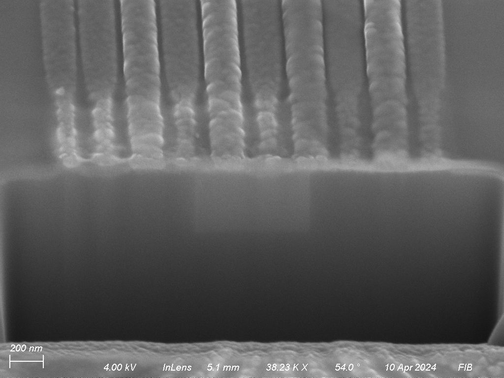
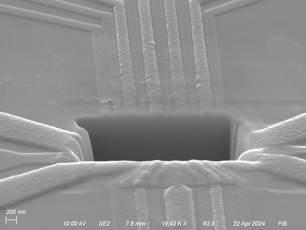
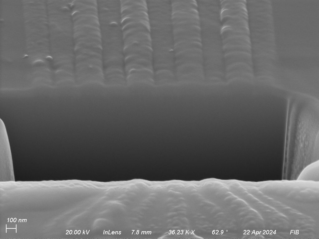
We used FIB to mill a approx. 3 µm width trapezium-shaped trench on the surface of Al gates to reveal the cross-sectional topography of gates. Using FIB to perform this task was a challenge since the Al gates are only few tens of nanometer thick and using high ion beam current can destroy the gate architecture.
Since the chip has simple planar geometry, tilting the chip while making sure that the region where we want to mill is eucentric wasn't much of a problem. At 54°, the feature was coincident with both SEM and FIB.
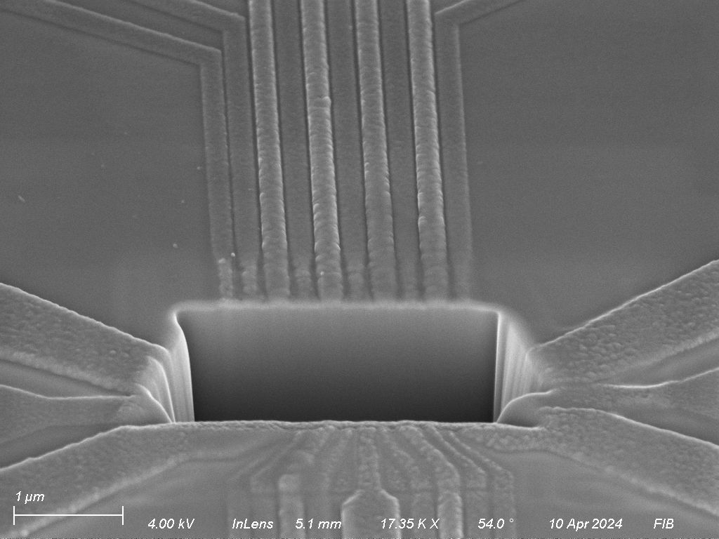
In the first run, we used 50 pA/30 kV aperture to mill the trapezoidal trench right at the gate overlapping region. The process was completed in two passes and the total time for the run was 180 seconds. The images obtained from this run are shown in Figure 13 and Figure 14.
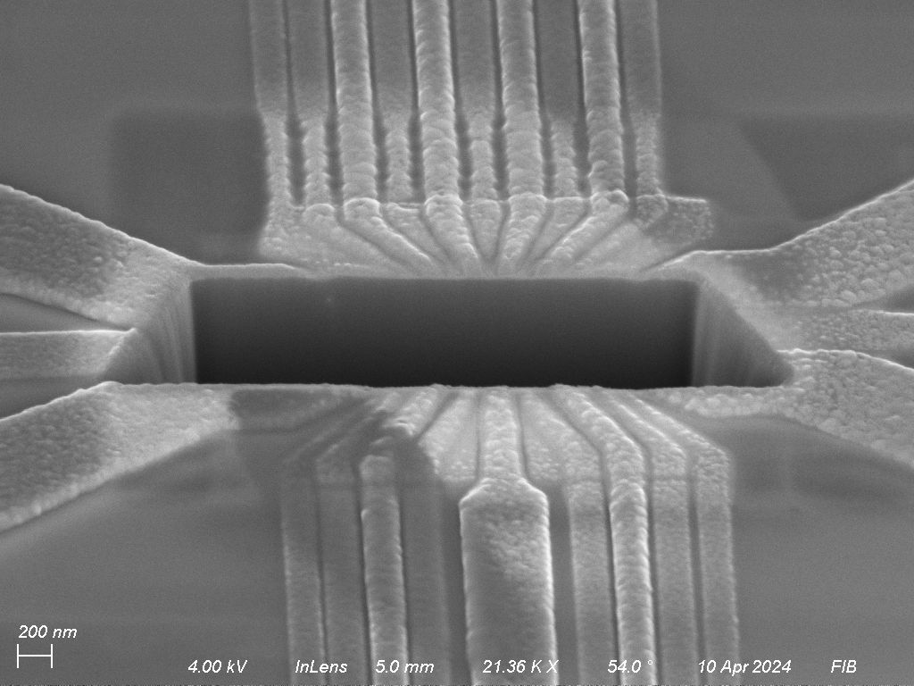
A higher magnification look at the region (Figure 14) shows that further milling is required to reveal the cross-section.

We characterized the silicon quantum dots using different EM techniques. We were also able to view the cross-section of Al gates but the morphology of the gates couldn't be viewed clearly. Future works can can explore other ways of revealing cross-sectional morphology.
Acknowledgments
I am sincerely grateful to Dr. Sean O'Neill for his continuous guidance and support throughout the project and his patience for training a beginner like me on EM techniques, especially FIB. I acknowledge Dr. John Nichol for the project idea. I am thankful to Nichol Group members for helpful discussions and support.
References
1. Mills, A.R., Zajac, D.M., Gullans, M.J. et al. Shuttling a single charge across a one-dimensional array of silicon quantum dots. Nat Commun 10, 1063 (2019). https://doi.org/10.1038/s41467-019-08970-z