![Piezoelectric effect[1]](piezoelectric effect.png)
Affiliation: Department of Physics and Astronomy, University of Rochester, New York 14627
Email: tzhang54@u.rochester.edu
Surface Acoustic Wave(SAW) Resonator is a useful electronic device which receives surface acoustic wave and convert such wave into electric signals. These resonators are integral components in various electronic devices, notably in signal processing and communication systems. The principle behind SAW involves the generation and detection of surface acoustics waves, such detection relies on piezoelectric material, typically quartz or lithium niobate. In our case, we use lithium niobate. These specific materials can generate electric charges when mechanically stressed, such phenomenon is called piezoelectric effect, which was discovered in 1880 by the brothers Pierre Curie and Jacques Curie.
As we can see in Figure 1, when piezoelectric material is stressed,
the crystal lattice distorts. The distortion changes the polarization of
the material by either increasing or decreasing the distances between
the positive and negative charges within the crystal. As a result, an
electric dipole is formed, leading to the appearance of an electrical
voltage across certain surfaces of the crystal. Conversely, when an
electric field is applied to a piezoelectric material, the field
influences the crystal lattice, causing it to change shape. In all, the
effect involves the conversion between electric energy and mechanical
energy.
Going back to the device itself, the resonator consists of several
parts: interdigital transducer and reflectors. Interdigital transducers
are the crucial part of the device, they can generate or detect surface
acoustic waves. A typical interdigital transducer consists of a series
of thin metallic electrodes. These electrodes are arranged in a pattern
such that alternating electrodes are connected together. The reflectors
on the device can help bounce the waves back and forth between them,
creating a standing wave pattern if the frequency of the input signal
matches the resonant frequency of the cavity formed by the
reflectors.
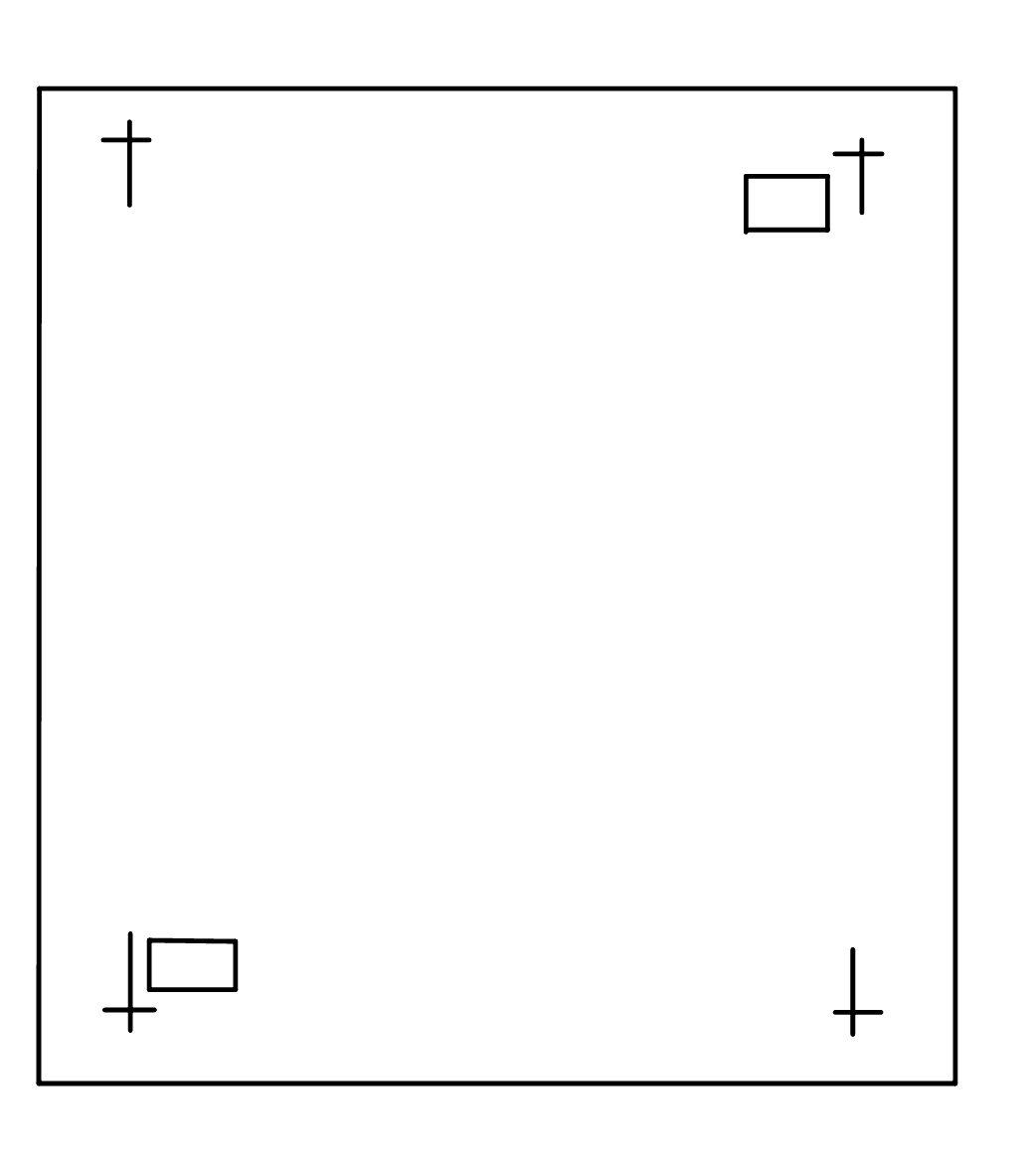
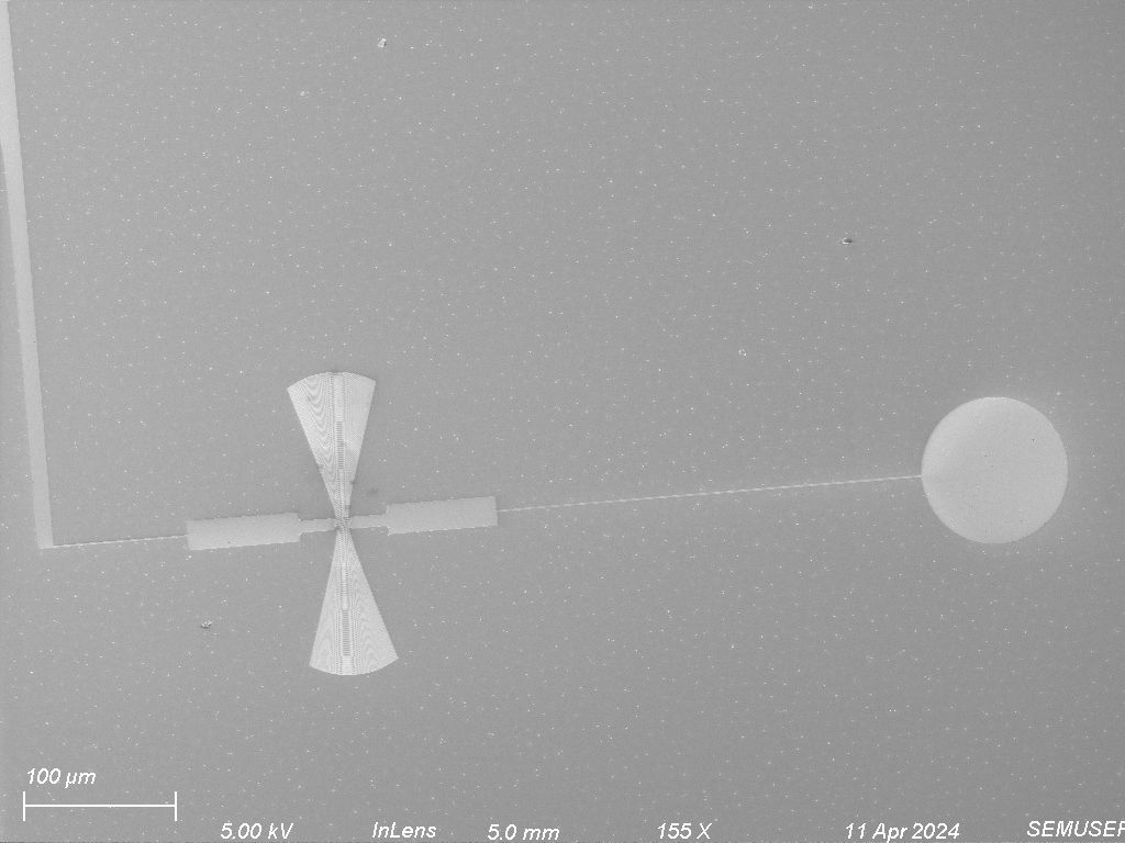
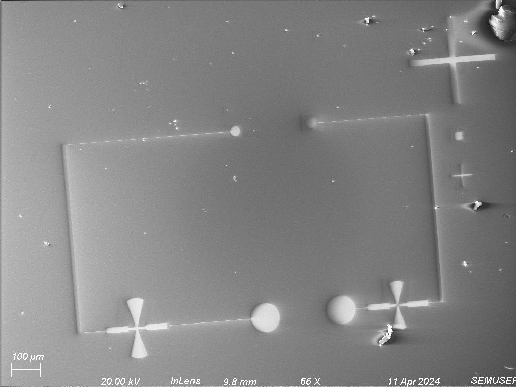
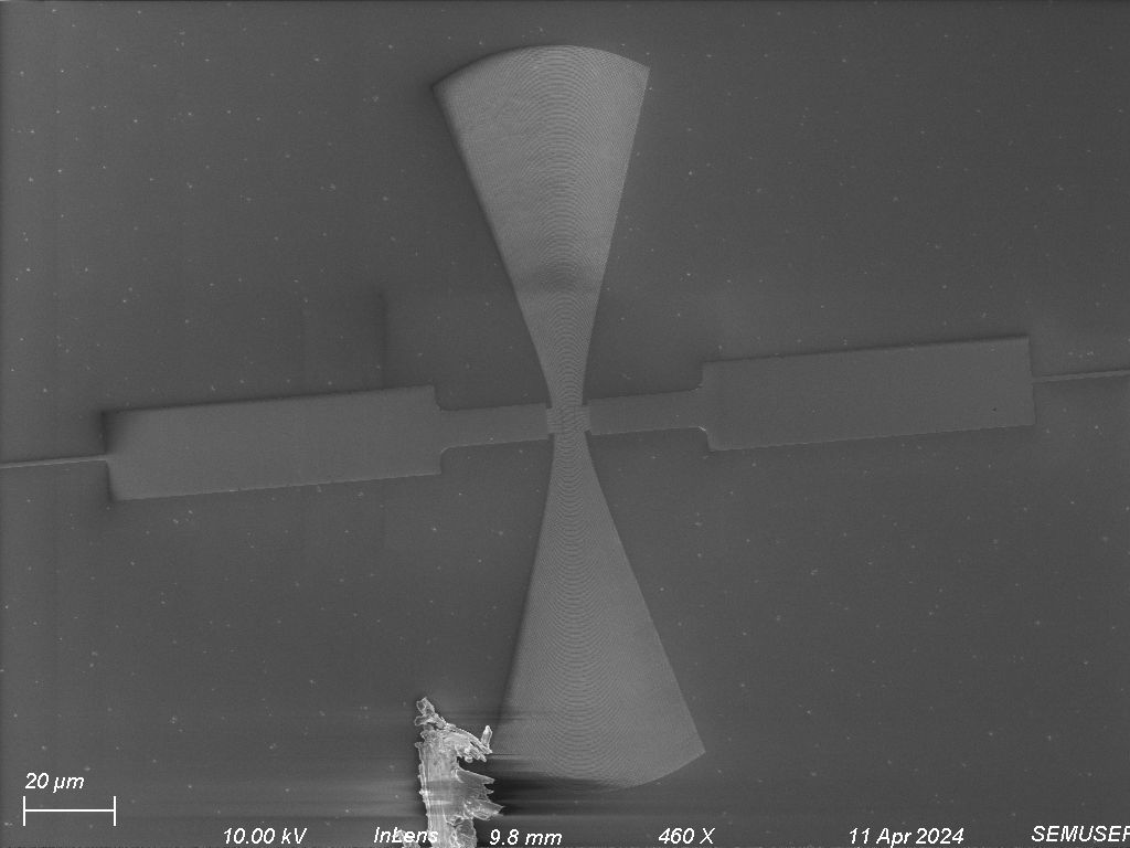
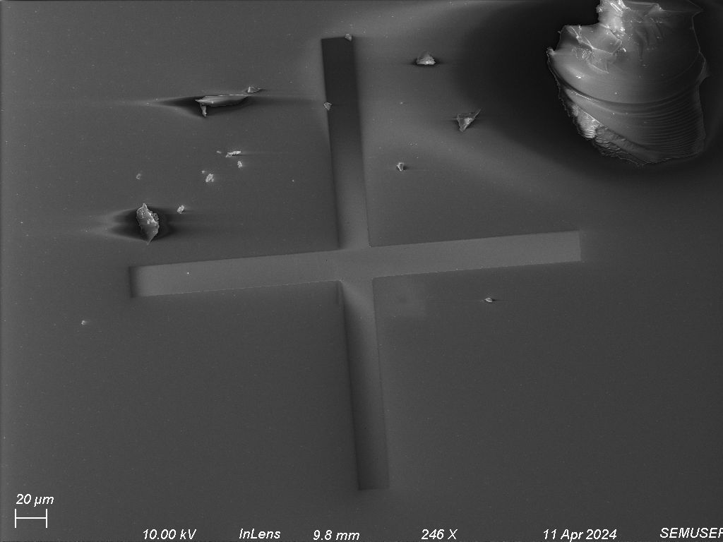
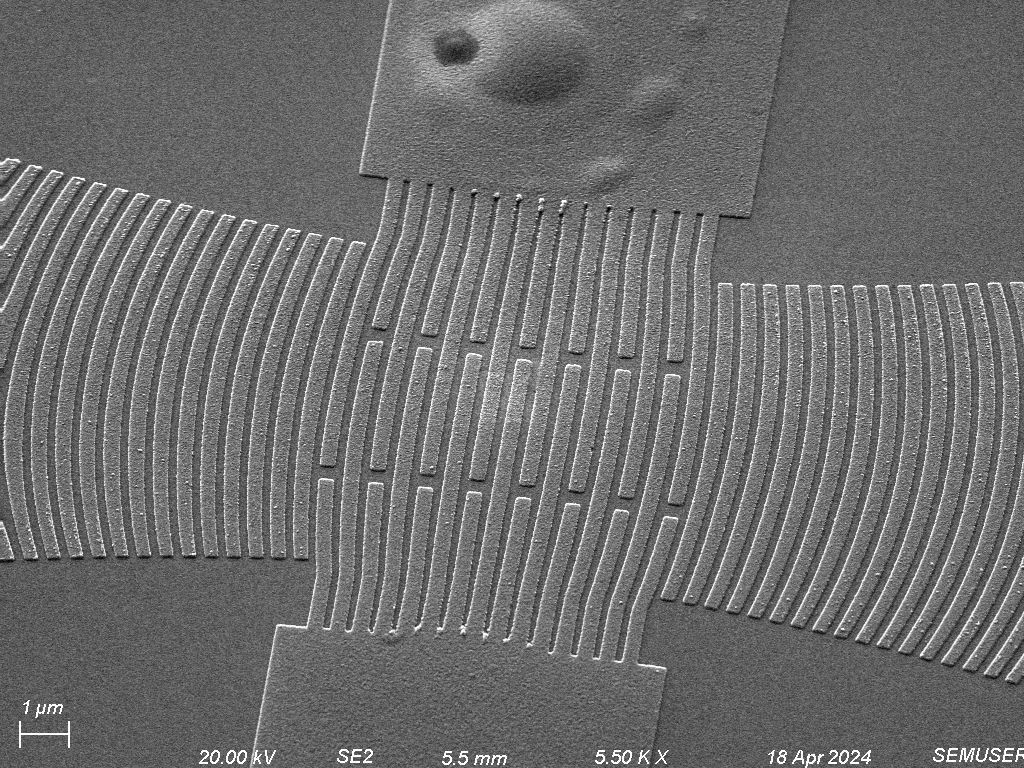
The layout of my sample is included in the previous figure. The
substrate is made of Lithium Niobate(\(LiNbO_3\)) and the electrodes are made of
aluminum. The crosses represent the reflectors and the squares represent
the interdigital transducer. The reflectors locate at the corners of the
sample, trapping the SAW of certain frequency. The sample is symmetrical
about the diagonal so if we reflect the specific pattern of interdigital
transducer on the top right about the diagonal, we get the one on the
bottom left.
After we know the mechanism behind electric signal generation, the last puzzle to complete the full picture is the resonance in the circuit. SAW resonators can very preciously select certain frequencies out of a complex signal, making them essential for mobile phones and radios. The process of selection is the process of resonance. The natural frequency of a SAW device refers to the frequency at which the device most efficiently converts electrical signals into acoustic waves (or vice versa). This frequency is determined primarily by the physical dimensions and properties of the IDT and the piezoelectric substrate. This sample is provided by Professor Nichol. The process of fabrication and physical properties are included. The resonance curve is shown below:
![Curve of resonance[2]](resonance.png)
We can also understand resonance by looking at a typical RLC circuit.
![RL circuit[3]](RL circuit.png)
![RLC circuit[3]](RLC circuit.png)
Let’s first consider a RL circuit, from Figure 4, we can write the following differential equation:
\[L\frac{dI}{dt}+RI=\epsilon_0 cos \omega t\]
Consider an alternating current:
\[I(t)= I_0cos(\omega t +\phi)\]
Input the current into equation(1).
\[-LI_0\omega (sin\omega tcos\phi +cos\omega t sin\phi)+ RI_0(cos\omega tcos\phi -sin\omega tsin\phi )=\epsilon _0cos\omega t\]
For the equation to hold, the constants of \(sin\omega t\) and \(cos\omega t\) should equal, and they gives:
\[-LI_0\omega cos\phi -RI_0sin\phi =0\] \[-LI_0\omega sin\phi +RI_0cos\phi - \epsilon_0=0\] \[tan\phi = -\frac{\omega L}{R}\]
And the equations above further indicates:
\[I_0 =\frac{\epsilon_0}{Rcos\phi -\omega Lsin\phi}=\frac{\epsilon_0}{R(cos\phi+an\phi sin\phi )}=\frac{\epsilon cos\phi}{R}\] \[cos\phi = \frac{\epsilon_0}{\sqrt{R^2+\omega^2L^2}}\]
And together, they gives: \[I_0 = \frac{\epsilon_0}{\sqrt{R^2+\omega^2L^2}}\]
Now, we move to the RLC circuit in Figure 5, different from RL circuit, now a capacitor is included. The equivalent \(\omega L\) term in RLC circuit is:
\[\omega L' =\omega L -\frac{1}{\omega C}\]
We take it back to the current and the final expression of the current \(I(t)\) is:
\[I(t)= \frac{\epsilon_0}{\sqrt{R^2+(\omega L-\frac{1}{\omega C}^2)}}cos(\omega t +\phi)\]
From the expression, and think when does the current be the greatest? Obviously, when the denominator is minimized. To decrease the denominator, we should make:
\[\omega L - \frac{1}{\omega C} = 0\] which indicates:
\[\omega_0 = \frac{1}{\sqrt{LC}}\]
Here the \(\omega_0\) is the natural frequency of the circuit. So when the driven frequency coincide with this frequency, the current in the circuit is maximized. With this example, we can also understand how surface acoustic wave resonator works in a filter in a cell phone/ radio. When a surface acoustic wave is received by the interdigital transducer, by piezoelectric effect, an alternating current of certain frequency will be generated by the device. If the generated current’s frequency is close or equal to the natural frequency, the current in the circuit will be maximized. Currents of other frequencies cannot achieve such high current. What we have to do is to set a high threshold current, if the current in the circuit exceeds the threshold, we know the device has detected a surface acoustic wave of the frequency we want. With this mechanism, the SAW resonator picks the wanted signal from a complex source.
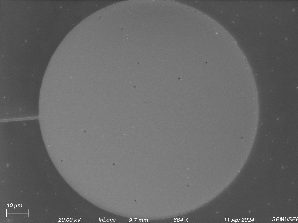
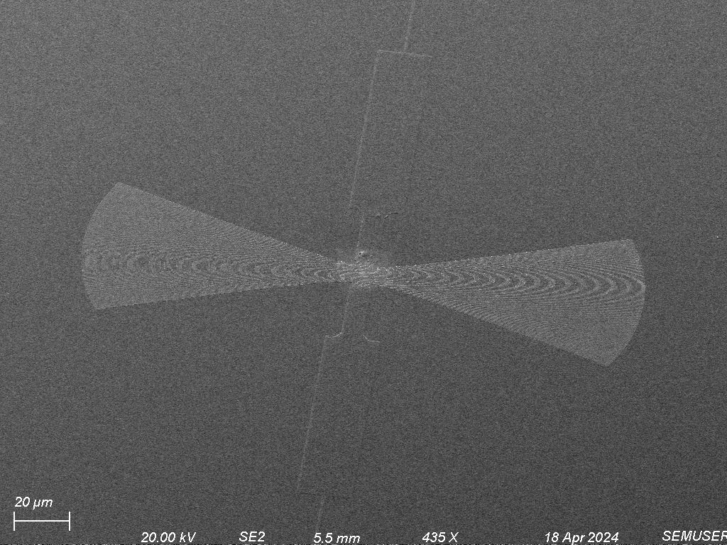
Apart from the boring theory part, let’s move to practical imaging. In the project, several imaging techniques were used to observe the sample. In the project, SEM, AFM and EDX were used to image the sample coated and uncoated. For the SEM, we mostly used InLens detector and a little secondary electron 2 detector. We didn’t use backscattered electron secondary electron 2 detector a lot is because with these detector, on the computer screen we cannot see a clear picture. The pattern is very unobvious.
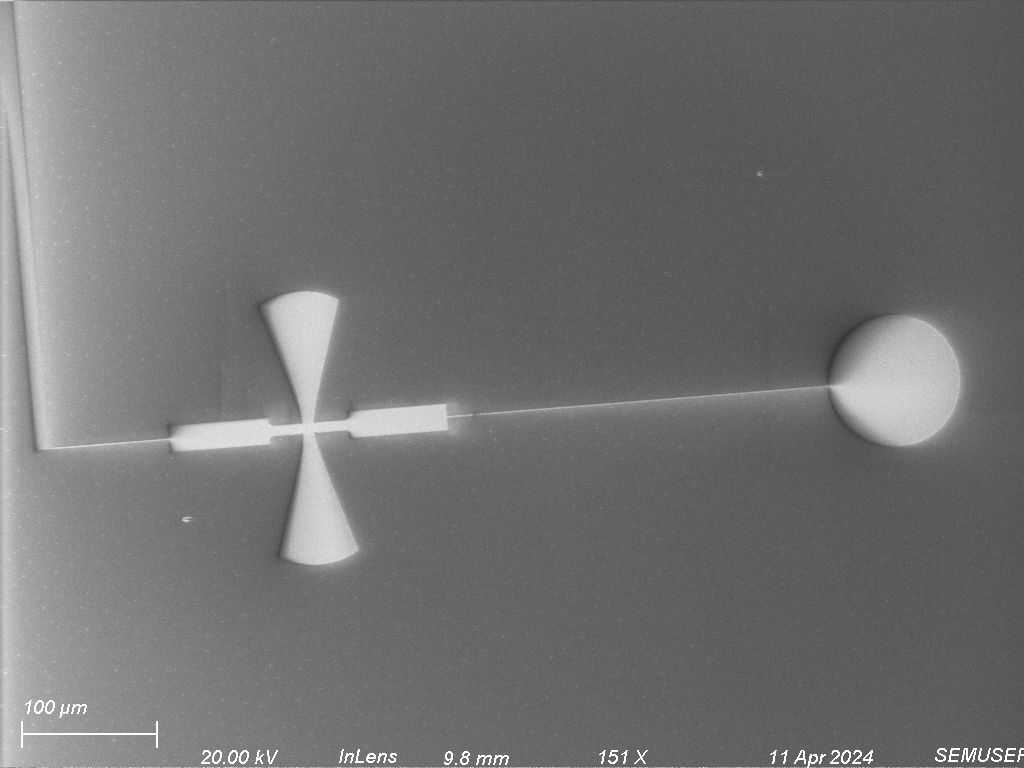
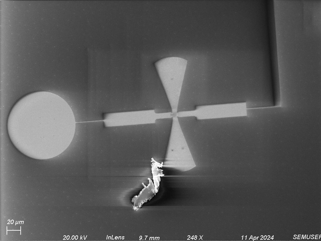
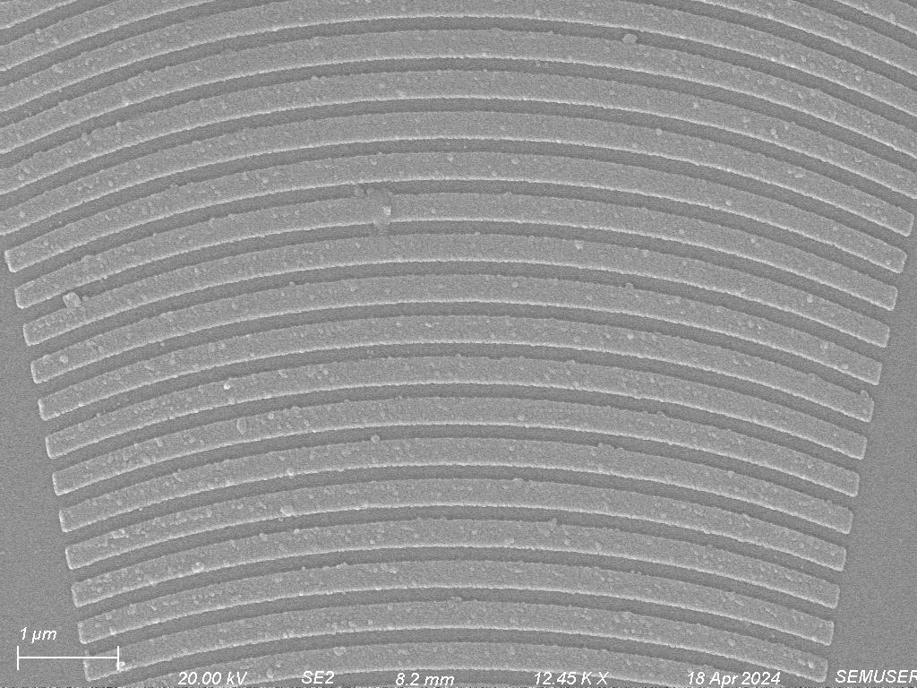
First, let’s take a general look at the interdigital transducer of the device:
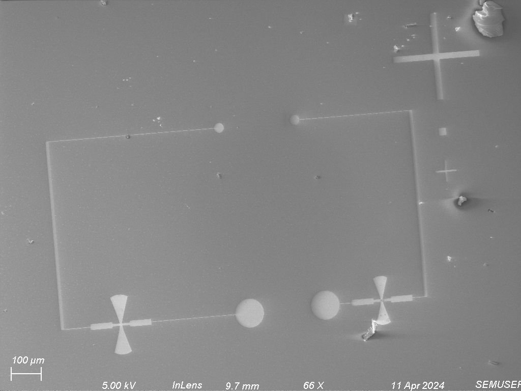
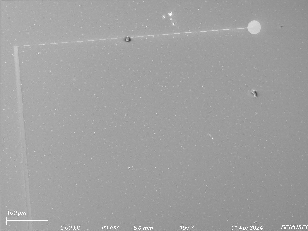
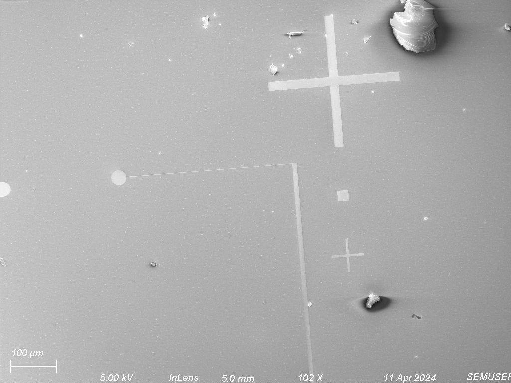
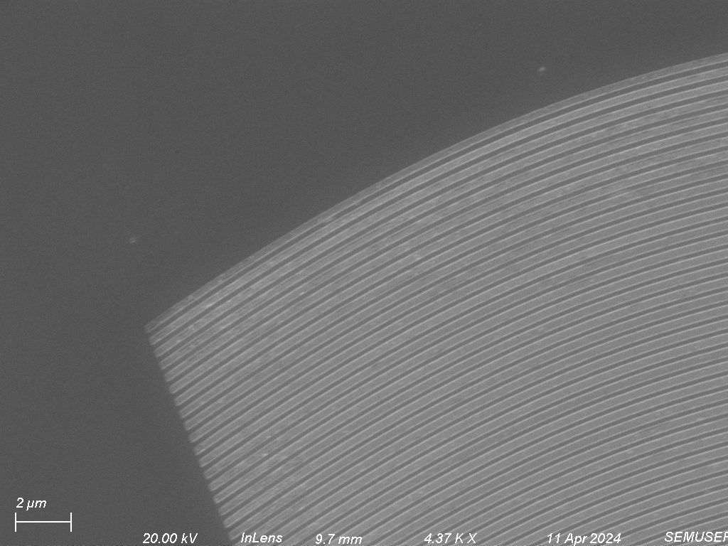
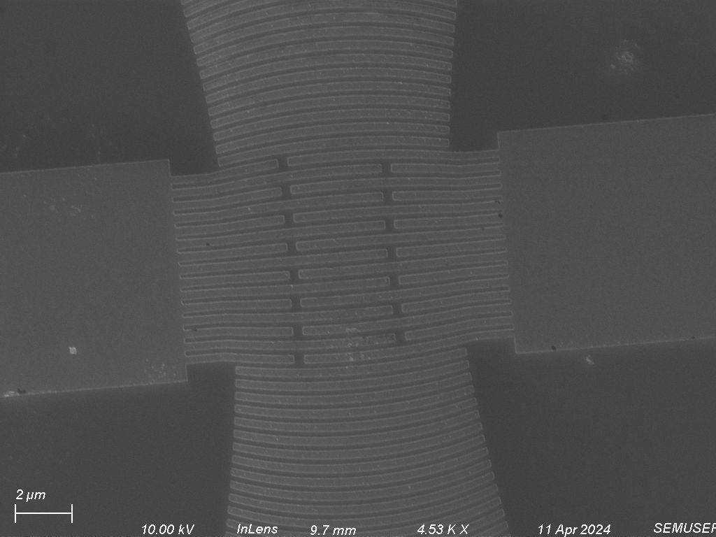
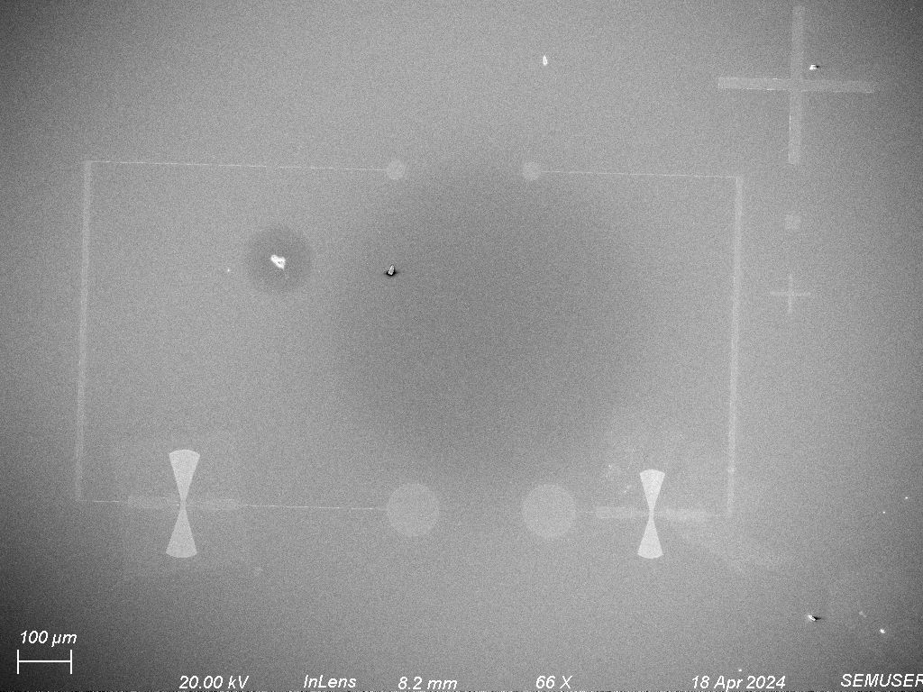
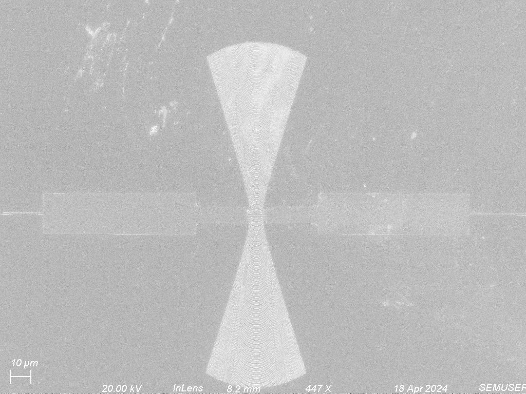
For the first two images, two general images were taken under different accelerating voltage. And the later four images take a closer look, each including a corner of the device.
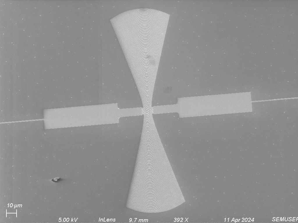
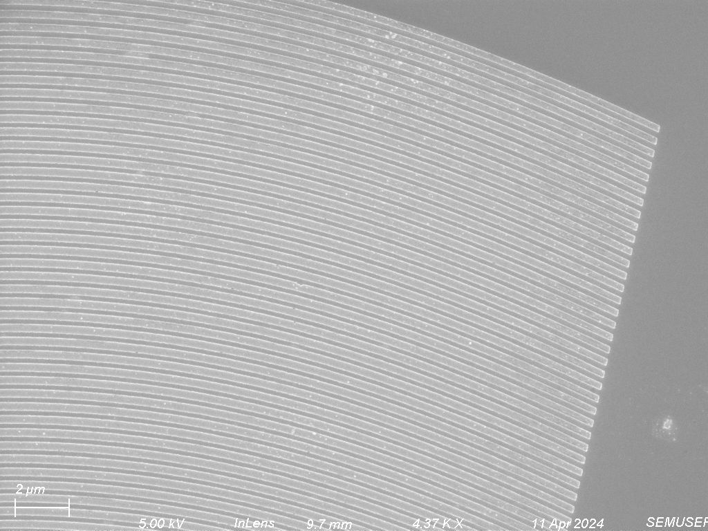
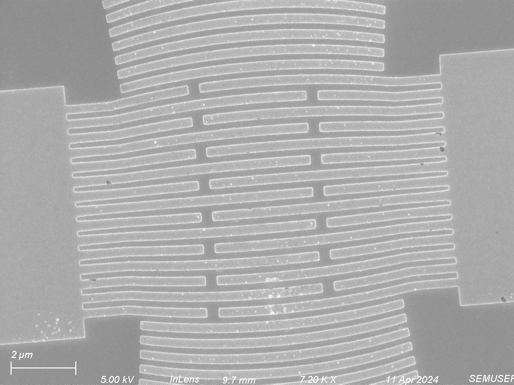
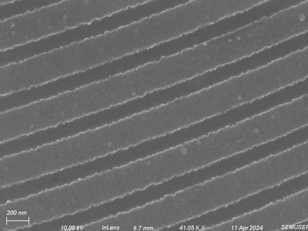
As we increase the magnification, in the first two images, we have
taken images of two specific device. The first one is the interdigital
transducer and the second one is the capacitor of the circuit. With
higher magnification, we can see the specific electrodes in the
interdigital transducer. What we can see is the upper and lower part
consists of arc of different lengths. In the middle, we have straight
electrodes going alternately. In Professor Nichol’s article, such mode
is called "Gaussian" Profile. Such profile’s response follow a gaussian
distribution and it also decrease the noise at the same time.[2]
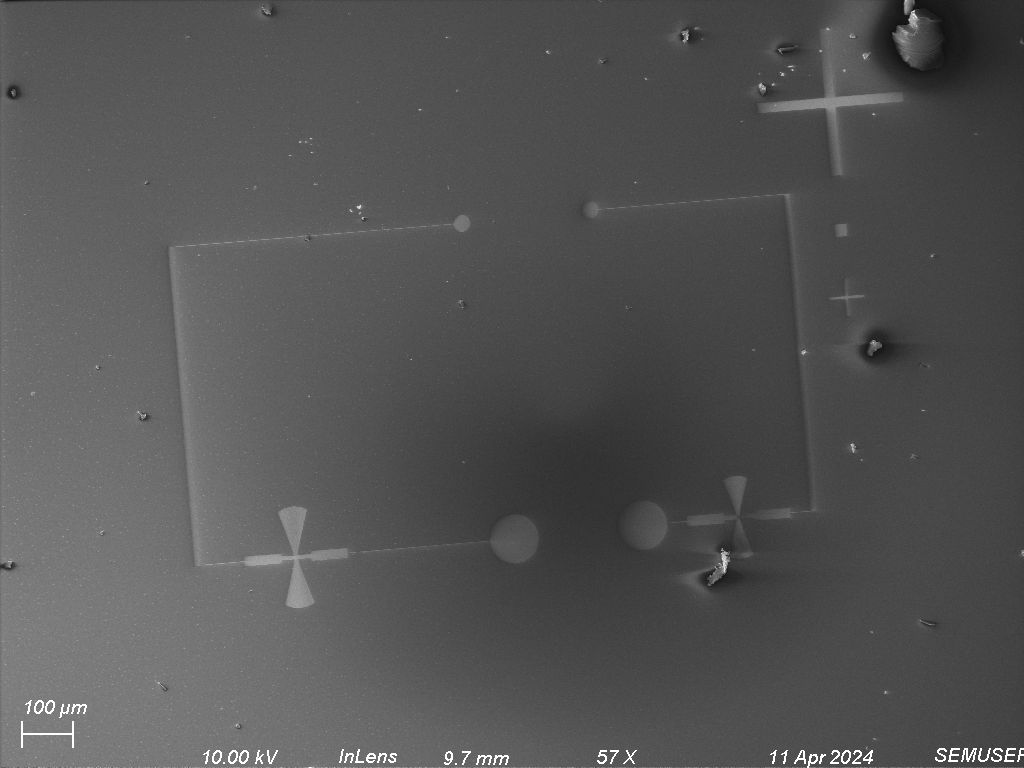
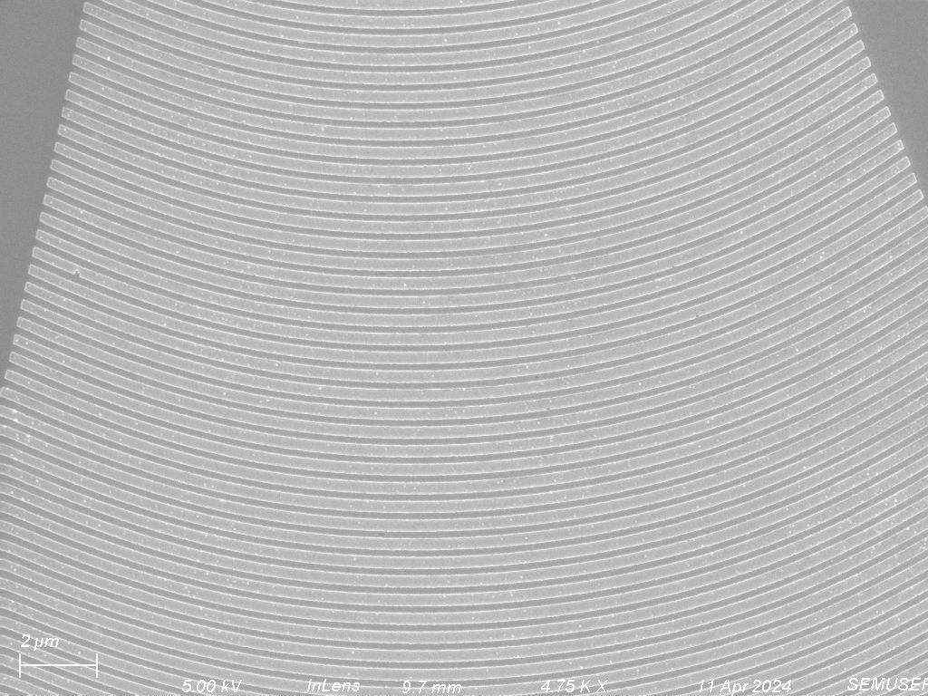
Next, the same images but with different accelerating voltage will be
displayed:
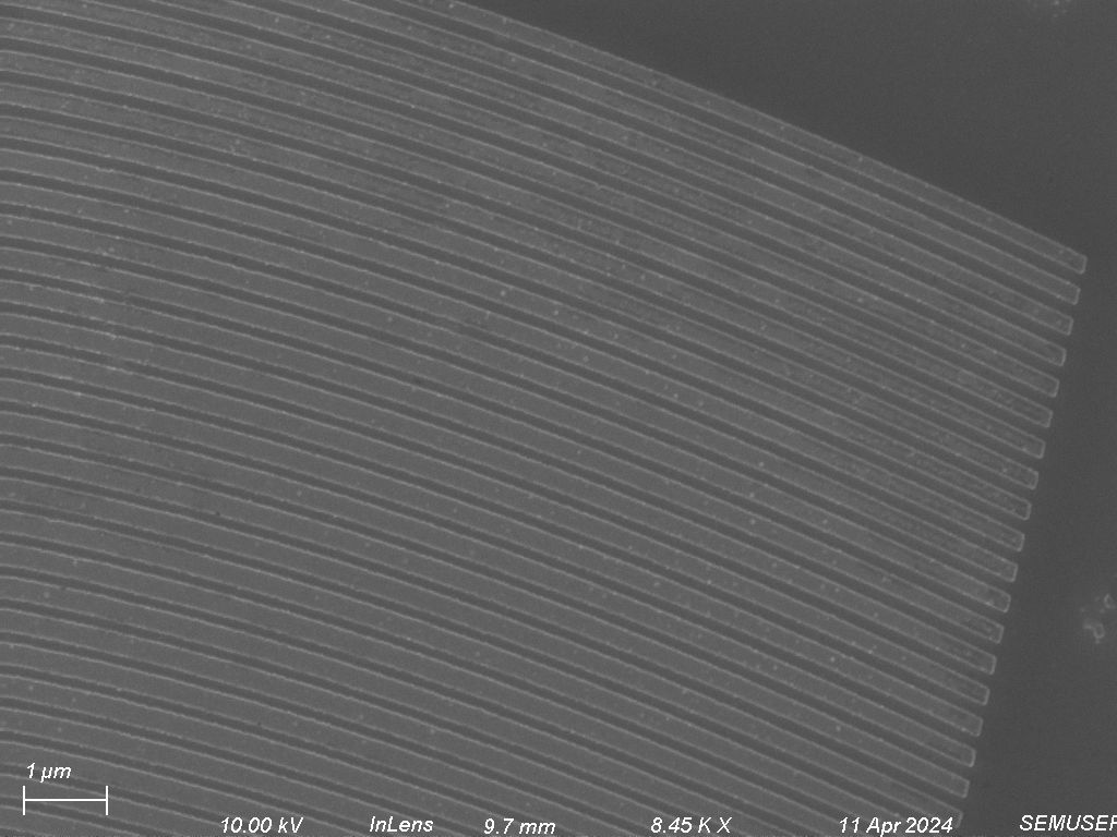
Theoretically, higher accelerating voltage means higher resolution, however, such effect is not obvious in the result. On the other hand, in the images, compared to the 5kV’s results, there are way more shading, implying the charging effect. For the impurities on the sample, they are obviously non-conductive, resulting those shadings. Another reason that 5kV works well is the structure we are observing are all on the surface of the sample. We have no need to dig into the internal structure of the sample. To further improve the result, we tried to sputter coat the sample with 50nm thick gold, and the results are shown below:
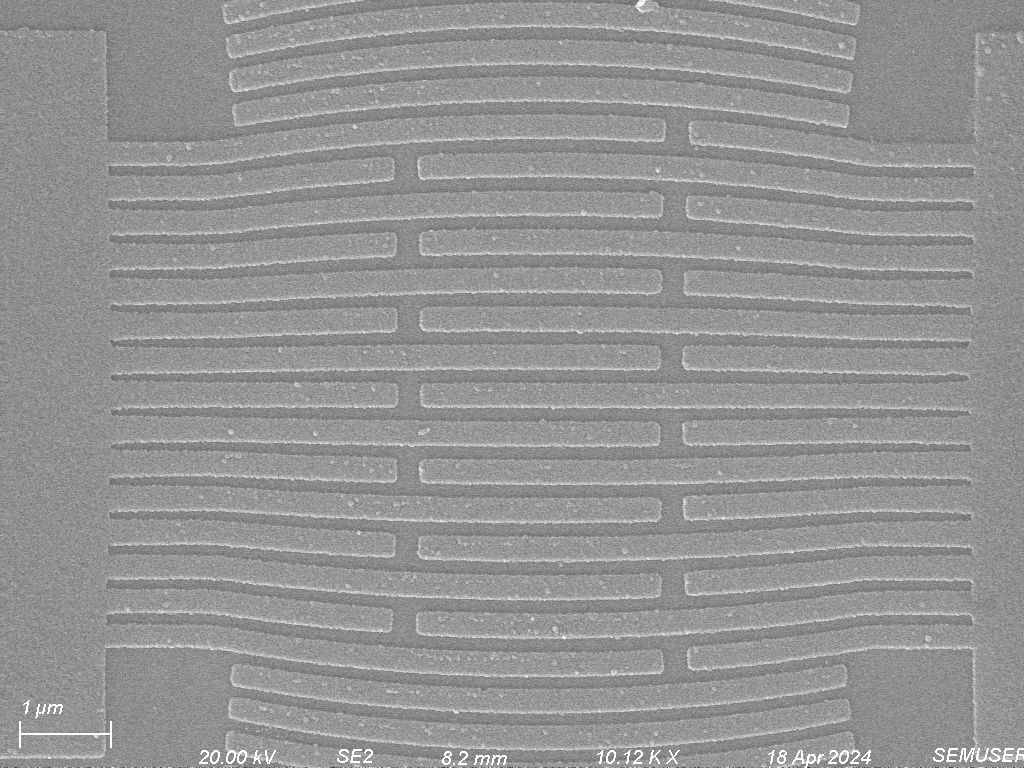
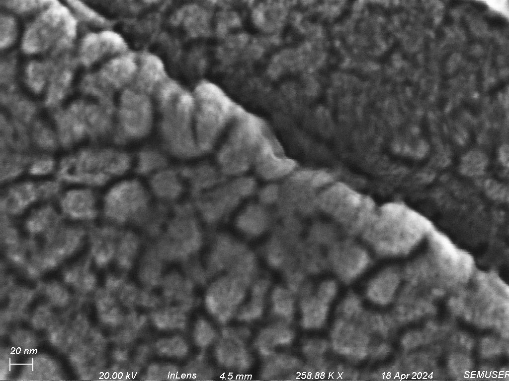
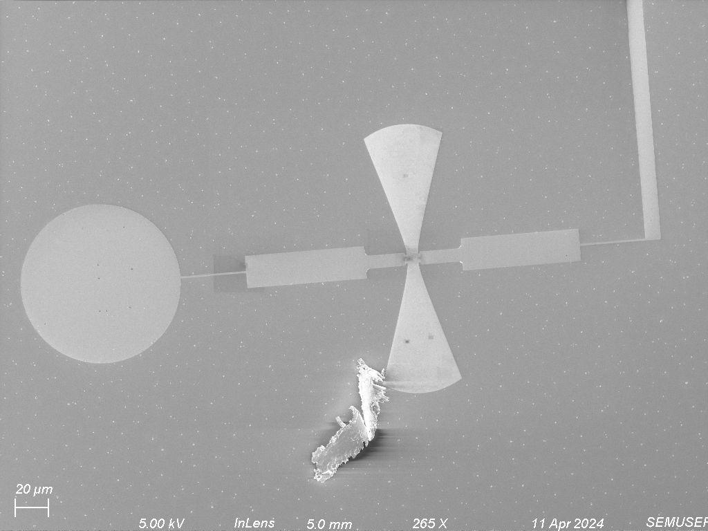
After coating, there are several observations: the first one is the image get much clearer. After ground the sample to the stage, the charging effect is reduced to the minimum. Also, when in high magnification to observe the interdigital transducer’s electrodes, the quality of the image gets much better. We can clearly see all the edges of the sample. We also took one image which goes into 250KX, showing the specific coating textures. However, when we are trying to take general images of the sample, the contrast became bad. We can hardly identify the device. The color of the edges almost fuses with the background. That phenomenon is caused by the coating material. We used gold, which is an element of high Z value. High Z atoms scatter electrons more strongly than elements with a lower atomic number, such as lithium. When electrons hit a gold-coated sample, they are more likely to be backscattered by the gold layer than they would be by a lithium substrate alone[4].
We also used AFM to see discover the topology of the surface of our sample. Two images with high resolution will be displayed. One is \(30\mu m * 30\mu m\), one is \(10\mu m * 10\mu m\). Since, the most intriguing, most complex part of our sample is the middle part of the interdigital transducer, which is the gaussian profile, the AFM focus on this region:
![RL circuit[3]](afm3030png.png)
![RLC circuit[3]](afm1010.png)
In image processing, we used polynomial fitting to fit the background of the result, making the background as flat as possible. We also polish the result to make the image clearer. In AFM we can view the pattern in 3D, which is a new perspective.
Lastly, we used EDX to carry out the elemental analysis to the sample. With EDX, we can see the elemental composition and distribution on the sample. First, here is the result of elemental composition:
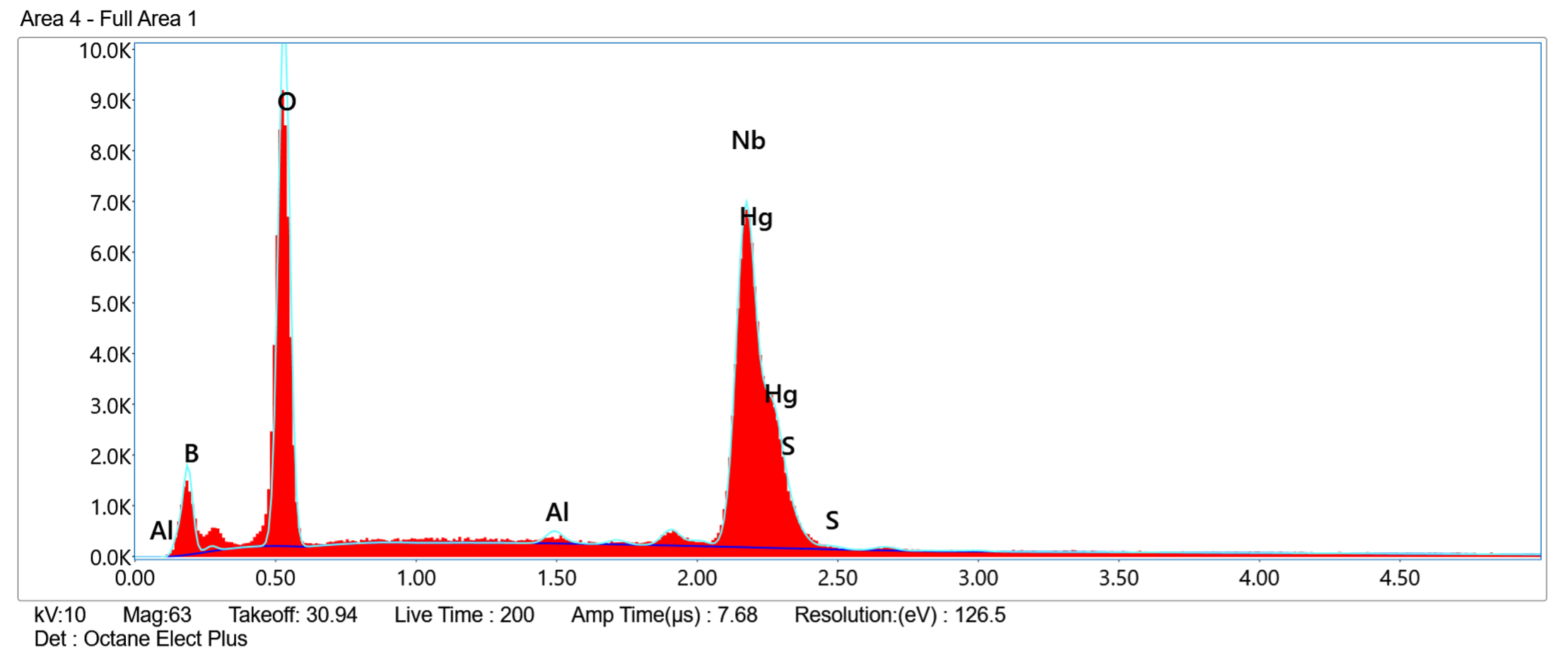
From the analysis, we can see that there are four main elements: carbon, oxygen, aluminum, and niobium. We can explain three of the elements, as we mentioned, the substrate is made of Lithium Niobate. EDX cannot detect Lithium because the element is too light. The electrodes are made of aluminum, we can see the results in the following multi-dimentional analysis.
![RL circuit[3]](milti1.png)
![RLC circuit[3]](milti2.png)
![RL circuit[3]](milti3.png)
![RLC circuit[3]](milti4.png)
From the results above. We can see that Carbon, Oxygen and Niobium distributes all over our sample. However, the result for Aluminum, although not clear, shows the shape of the circuit. The signal is very weak, partially due to the time taken is relatively short, partially due to the quantity of atoms is small. If you take a close look at the image, you can see the general shape of the circuit, the rectangular shape. And on the top right, there is a cross, which is the reflector on the top right of the circuit. The results of EDX further confirmed that the substrate is made of Lithium NIiobate and the electrodes are made of Aluminum.
In the project, we first explained the theory of our device to ensure a solid foundation. We also used several imaging techniques: SEM, AFM and EDX to analyze the sample. Each technique provides a perspective, having their own advantages and disadvantages. By combining them together, we get a comprehensive understanding to our sample, the Surface Acoustic Wave Resonator.
The Author would like to thank John Nichol for providing the sample. Thanks to Sean O’Neill and Gregory Madejski for their help on AFM, EDX and SEM training and their supervision during the project. The author would also like to thank his parents for their genuine support during the project.