Department of Electrical and Computer Science, University of Rochester, Rochester, NY, 14627
Introduction
In the field of nanoelectronic fabrication, EBL ( e-beam lithography or Nanometer Pattern Generation System ) is widely used due to its precise patterning of nanometer-scale features on substrates. It stands out as it is capable to achieve higher resolution than photon lithography. In EBL, a layer of resist is exposed to the electron beam. The electron beam can break the polymer chains (chemcial chains in the resist) into small pieces which makes it more disolvable in the developer solution.
The resolution of pattern depends on various factors. In this project, the effect of accelerating beam voltage is discussed while other parameters, including beam source aperture, the shape of pattern, the amount of dose and the material of the chip remain unchanged.
The effect of the accelerating voltage on the pattern is quantified by the minimum feature size and the depth of the pattern.
The electrons do forward scattering in the resist (PMMA). The main parameter that impacts the interaction volume is energy (the density and material of the resist remain unchanged) which is the accelerating voltage of the electron beam. Higher accelerating voltage tends to result in larger interaction volume. The BSEs (backscatter electrons) resulted from the elastic collision between the electron beam and the sample mostly penetrate the PMMA layer into the silicon substrate. The SEs (secondary electrons),resulted from the inelastic collision, meanwhile, generated closer to the surface of the PMMA layer which are the major contributor to the resist exposure. The number of SEs depends on the size of interaction volume which is a proportional to the accelerating beam voltage in this case. In this case, the resolution is expected to be finer under high voltage as more SEs generated which the minimum feature size is smaller.
Under high accelerating voltage, the electron beam is expected to penetrated deeper in the silicon substrate. With large interaction volume generated, the SEs are expected to be generated from greater depth from the surface than cases under low voltage. In other words, the depth of the pattern increases with the accelerating voltage. This is verified by Monte Carlo Simulation of ElectroN Trajectory in SOlids (CASINOS) and measurement from atomic force microscope (AFM).
Fabrication
The model of SEM (scanning electron microscope) used in this lab is Zeiss Auriga Scanning Electron Microscope with NPGS attached to it.
The variables of the EBL other than accelerating beam voltage are pre-set as following
Beam source aperture: 30μm
Dose/area: 750 μC/nm2
Material of the chip: silicon substrate with 100nm PMMA layer.
Size of the chip: 5mm × 5mm
Accelerating Voltage: 20keV, 15keV, 10keV
Sputter Coating: 5nm Au
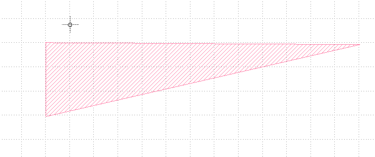
To test the minimum feature size of the EBL tool, a triangular pattern is fabricated on a blank chip. The pattern is drawn by Klayout.
Figure 1: The Triangular Pattern Designed in Klayout: 100μm in length and 20μm in height
A proper operating range of accelerating voltage for EBL is 10keV to 100keV .
The maximum limit of the SEM tool is 20keV. Therefore,with the setting given in the previous section, the accelerating beam voltages are selected to be 20keV, 15keV, and 10keV.
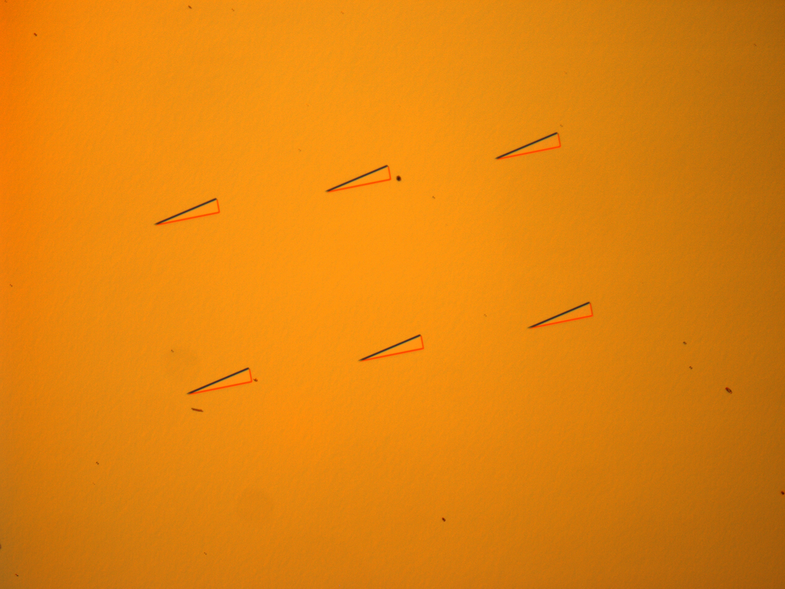
Since the pattern is tiny compared with the size of the chip, a run file is created in the NPGS software that repeatedly draws the pattern as a 2×3 array which allows the pattern to take more significant area on the chip.
To ensure the pattern has been successfully carved on the chip, light microscope is used to observe and locate the pattern on the chip after development.
Observation under Microscope
Figure 2: Pattern under Light Microscope.
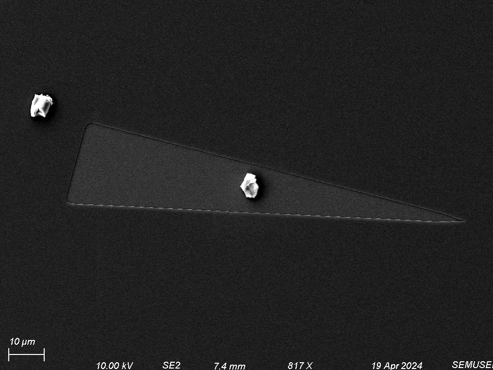
As the location of the pattern is found out, the sample is loaded into SEM and observed. Inlens imaging mode is used.
Figure 3: Pattern under SEM. The white dot is a dust on the chip
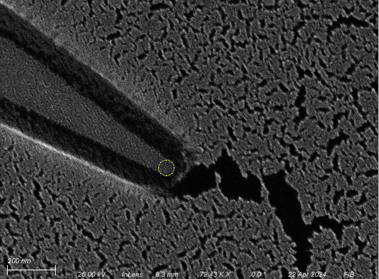
Scanning Electron Microscope: Minimum Feature Size
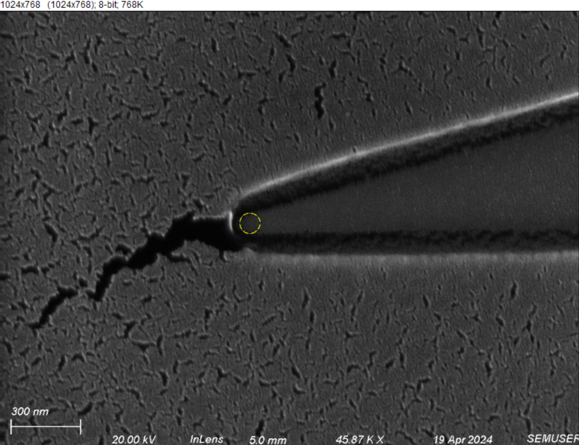
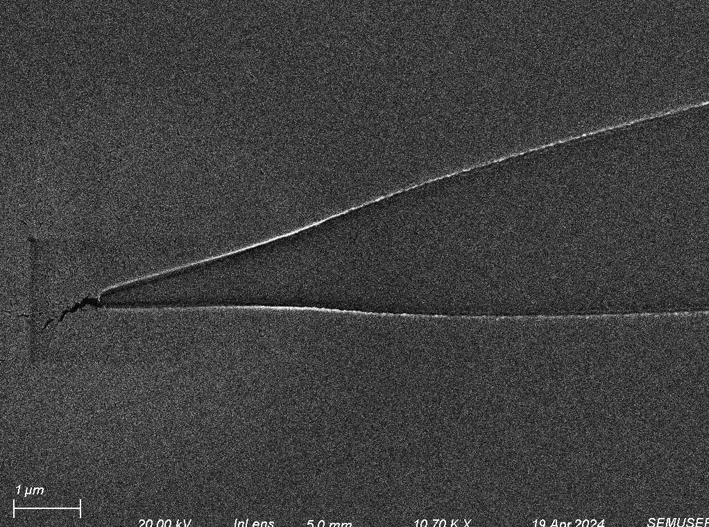
The minimum feature size here is determined by the sharpness of the smallest angle of the triangular pattern. The sharpness is measured by the diameter of the circle drawn by ImageJ that just fits the edge the triangle. The sample is sputter coated with 5nm gold before loading into SEM for better imaging.
Pattern with 20keV, the minimum feature size: 64.88nm
Pattern with 15keV, the minimum feature size is 76.17nm
Pattern with 10keV, minimum feature size: 90.61nm
Pattern with 10keV. Fistortion is observed under low magnification
As the recorded data shows, the minimum feature size is small when implement high accelerating voltage.
Since the EBL tool is not able to resolve finer feature beyond its limits, cracks are left in the front of the edge which represents the unfinished drawing of the edge.
Same with prediction, the higher accelerating beam voltage leaves shorter crack as fewer unfinished portion of edge which also lead to the conclusion that higher accelerating voltage results finer feature.
CASINO Simulation : Pattern Depth
The pattern depth is firstly simulated by Monte Carlo simulation of electron trajectories (CASINOS) to predict the effect of the accelerating voltage on the pattern depth.
CASINO Energy Distribution: 15keV
CASINO Energy Distribution: 20keV
It is clear that, under 20keV, the backscatter electrons penetrate more than 3000 nm into the silicon substrate while, under 15keV, the BSEs only penetrate 2000 nm into the silicon substrate.
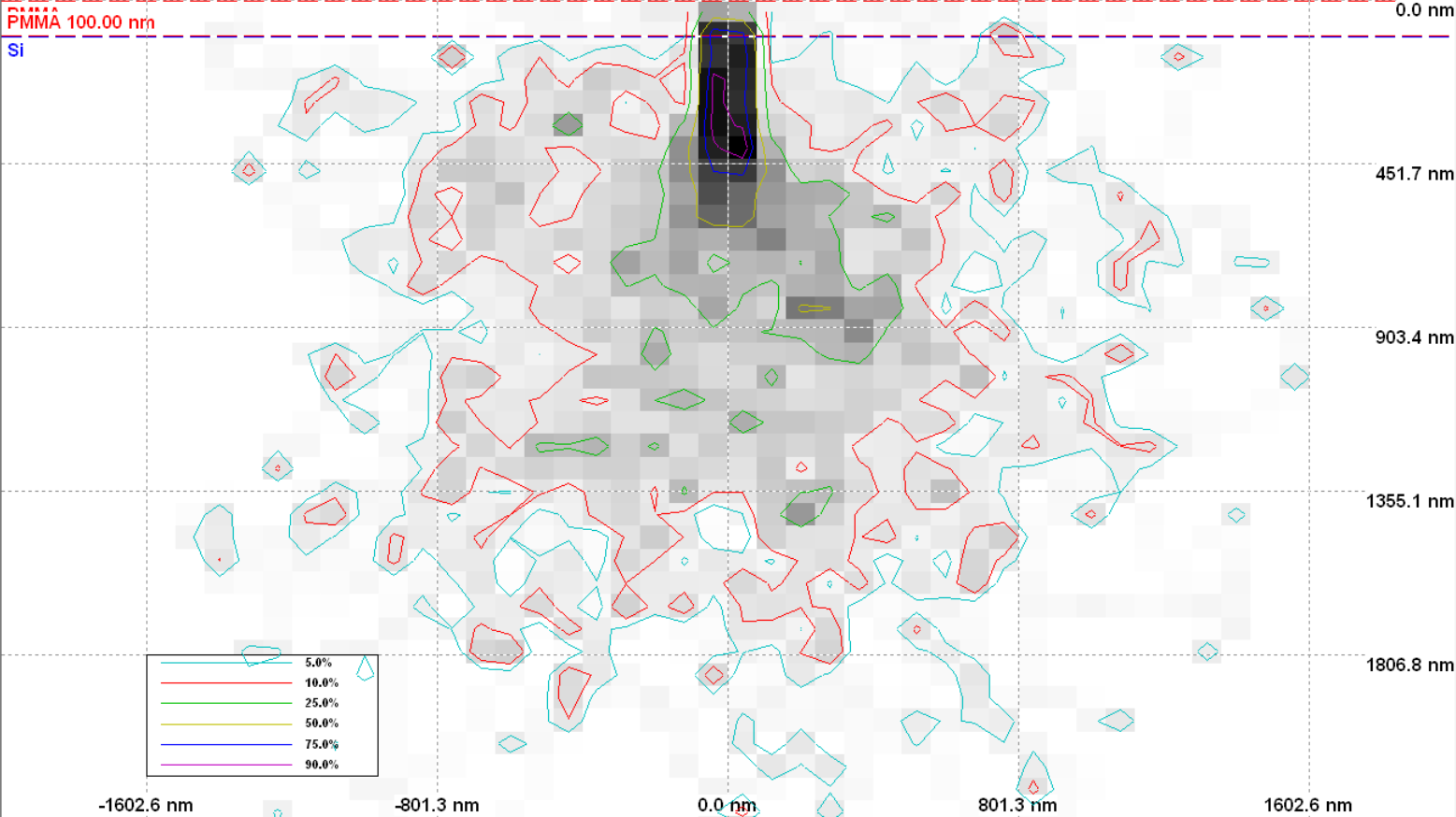
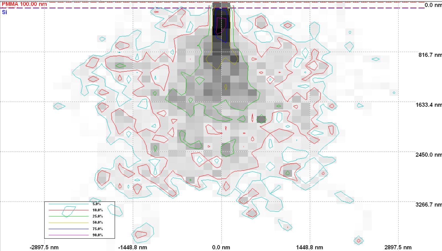
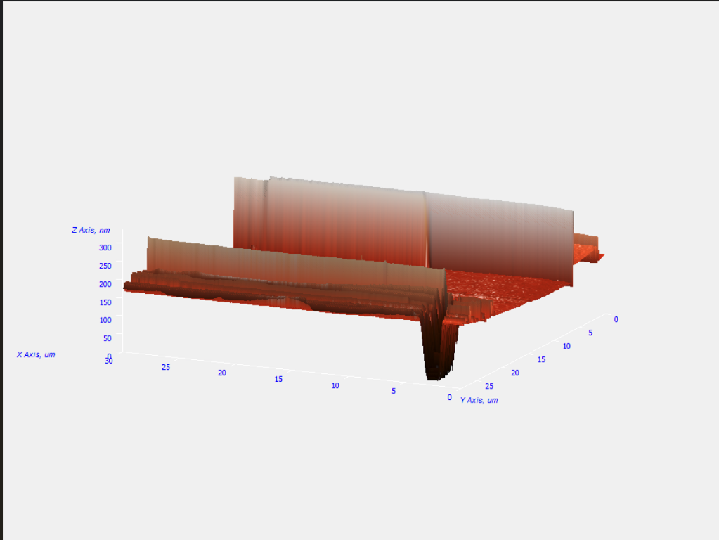
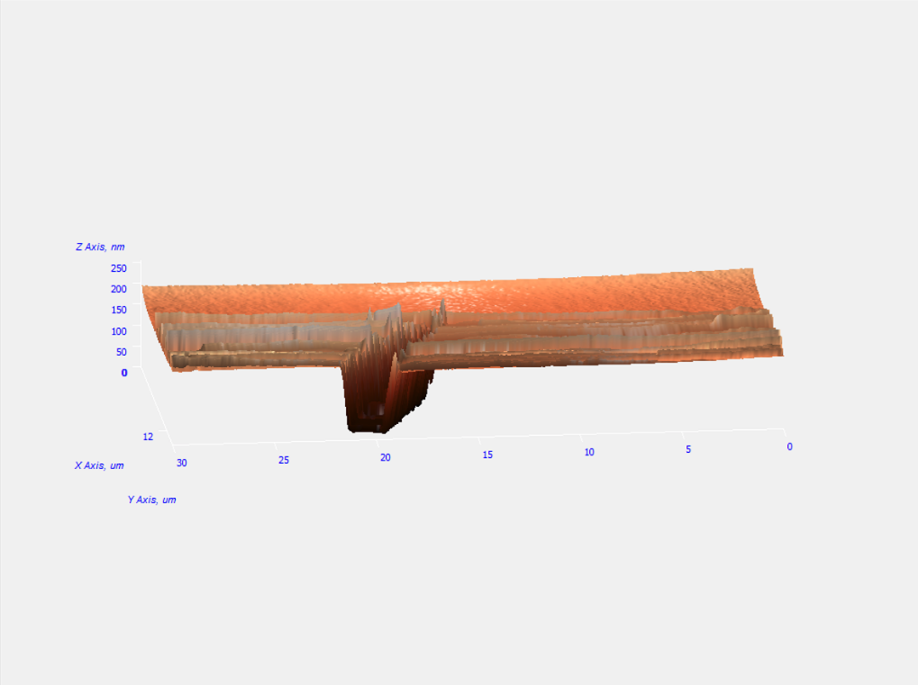
The model of the AFM is NTMDT AFM Microscope. The actual depth of the pattern is measured by the AFM. Only the smallest angle of the triangular pattern is scanned under AFM.
AFM 3D Model: 15keV
AFM 3D Model: 20keV
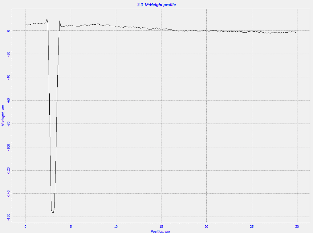
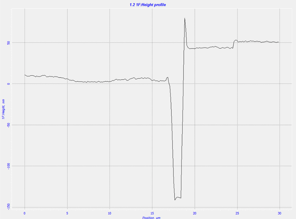
The precise depth is shown by the height profile data
Height Profile with 15keV. Depth = 168.38nm
Height Profile with 20keV. Depth = 180nm
Since the scan rate is large, the graphs are distorted. However, the difference between the pattern depth of two accelerating voltage is large enough to be viewed.
Conclusion
The SEM results reveal the dependency of the minimum feature size over the accelerating beam voltage. Higher accelerating beam voltage tends to yield better resolution pattern. The AFM and CASINOS reveal that higher accelerating beam voltage can yield pattern with greater depth.