Microscopy Characterization of Nano-Scratch Damage on Hafnia & Silica Multilayers
Matthew Hum, M.S.
Materials Science Graduate Program, University of Rochester
Nano-scratch testing was performed on two dielectric multilayer thin-film stacks—SiO2 -on-HfO2 and HfO2-on-SiO2 —deposited on fused silica substrates to evaluate mechanical durability and interfacial failure behavior. Multimodal characterization techniques, including optical microscopy, low- and high- voltage SEM, EDS mapping, AFM topography analysis, and electron interaction simulations, were used to assess surface damage, material ablation, and compositional transitions. The results revealed full- layer delamination and localized substrate exposure in both configurations, with more severe charging and brittle fracture behavior observed in the HfO2-top sample. High-resolution SEM and EDS data confirmed sequential layer removal during mechanical loading. AFM imaging of non-scratched regions established baseline flatness and demonstrated higher intrinsic surface roughness in HfO2 films. These findings provide insight into mechanical failure mechanisms of dielectric stacks and underscore the importance of top-layer material properties in multilayer durability under mechanical stress.
I. Introduction
Multilayer dielectric thin films comprising alternating layers of SiO2 and HfO2 are widely used in optical coatings, microelectronics, and MEMS due to their high dielectric constants, me- chanical hardness, and optical transparency. However, their mechanical durability—particularly under localized stress conditions such as contact or abrasion—remains a critical performance metric. Understanding how layer sequence affects damage tolerance and interfacial failure is essential for improving reliability in practical applications. In this study, nano-scratch testing was employed to probe surface integrity and damage propagation in two different multilayer stacks: one with SiO2 as the top layer and another with HfO2 on top, both deposited on fused silica substrates. Using a combination of advanced surface characterization techniques, including
SEM, AFM, EDS, and modeling of electron interaction volumes, we analyzed the effects of top- layer material, layer sequence, and interfacial properties on mechanical response and failure modes.
II. Materials and Methods
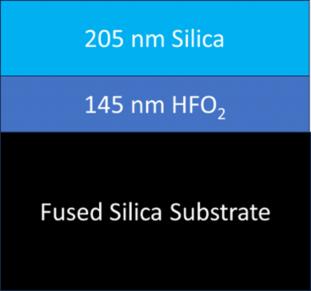
To investigate the mechanical durability and failure mechanisms of dielectric multilayers under nano-scratch conditions, two film stacks that were pre-scratched with a diamond tip were provided by D. Broege and J.C. Lambropoulos from the Laboratory for Laser Energetics (LLE). Both stacks consist of alternating layers of hafnium dioxide (HfO2) and silicon dioxide (SiO2 ), common high-index and low-index dielectric materials used in optical coatings and microelectronic applications. The first sample, referred to as the Silica-Top Sample, comprises a 205 nm thick layer of SiO2 deposited atop a 145 nm thick HfO2 layer. The second configuration, termed the Hafnia-Top Sample, inverts this architecture, featuring 145 nm of HfO2 as the top layer above a 205 nm SiO2 layer. In both cases, the bilayer structure is supported by a transparent fused silica substrate, chosen for its chemical stability and optical clarity. These contrasting layer sequences enable direct comparison of surface response and failure onset as a function of top- layer material during mechanical stress testing.
Figure 1. Cross-sectional schematic of the Silica-Top Sample showing 205 nm SiO2 atop 145 nm HfO2 on a fused silica substrate.
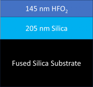
Figure 2. Cross-sectional schematic of the Hafnia-Top Sample showing 145 nm HfO2 atop 205 nm SiO2 on a fused silica substrate.
A multimodal characterization strategy was employed to assess scratch-induced damage and material removal in the multilayer thin film stacks. Optical microscopy in Nomarski differential interference contrast (DIC) mode was first used to visualize surface defects and delamination with enhanced contrast. Scanning electron microscopy (SEM) was conducted at both low (2 keV) and high (16 keV) electron beam energies to capture fine surface morphology and to facilitate elemental analysis via energy-dispersive X-ray spectroscopy (EDS). The low-energy mode minimized surface charging artifacts, while the high-energy mode enabled excitation of characteristic X-ray lines, particularly for hafnium (Hf). For the HfO2-top sample, a blue-color SEM image was generated using post-processing techniques to visually enhance layer boundaries and surface damage contrast along the scratch path. To investigate non-scratched surface integrity, atomic force microscopy (AFM) was performed, confirming baseline flatness and homogeneity. Additionally, an electron flight simulator was used to model interaction volumes and electron penetration depth during 16 keV SEM imaging, verifying suitability for deep layer analysis.
III. RESULTS
Differential interference contrast (DIC) optical microscopy was used to assess surface damage and scratch morphology in both multilayer samples. The enhanced contrast provided by Nomarski
imaging revealed distinct failure characteristics associated with the top-layer material. In the Silica-top sample, the scratch track displayed extensive surface cracking, lateral delamination, and regions of partial layer detachment. Iridescent interference fringes surrounding the scratch suggest localized stress accumulation and shear deformation at the SiO2 /HfO2 interface. In contrast, the Hafnia-top sample exhibited more pronounced material pile-up along the scratch edges and broader zones of apparent top-layer displacement, indicative of brittle fracture behavior in the HfO2 layer. The severity and width of the damage zone were greater in the Hafnia-top sample, which may reflect differences in mechanical compliance and interfacial adhesion between the two configurations. These optical findings corroborate later SEM and EDS evidence of layer ablation and differential layer failure behavior.
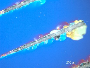
Figure 3. Nomarski DIC optical micrograph of the Silica-top sample after nano-scratch testing. The image shows linear scratch paths with adjacent lateral delamination and surface cracking. Color fringes indicate local stress and thin film interference effects, particularly at the SiO2 /HfO2 interface.
Monte Carlo simulations were conducted via Electron Flight Simulator (EFS) to model electron interaction volumes within the multilayer stacks under high-energy SEM conditions. A beam energy of 16 keV was selected to ensure adequate excitation of elemental X-ray lines for EDS, particularly the Hf Lα and Kα peaks. The simulations revealed significant differences in penetration profiles between the two sample configurations. In the Silica-top sample, electrons exhibited deep overpenetration beyond the 205 nm SiO2 and 145 nm HfO2 layers, reaching into the fused silica substrate. This suggests that despite silica’s lower atomic number and density, it provides minimal beam attenuation at this energy. In the Hafnia-top sample, the denser HfO2
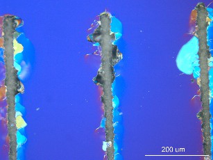
Figure 4. Nomarski DIC optical micrograph of the Hafnia-top sample after nano-scratch testing. Compared to the silica-top sample, the damage zones are wider with more pronounced edge deformation and material pile-up, characteristic of brittle failure in the HfO2 top layer.
layer absorbed more energy initially, but the overall interaction volume still extended into the underlying SiO2 and substrate. The hemispherical spread and depth of penetration in both cases confirm that surface charging is likely, especially in dielectric materials with low conductivity such as HfO2. Nonetheless, this acceleration voltage is necessary to excite deeper energy shells and to accurately detect interfacial composition using EDS.
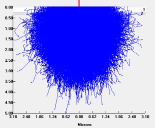
Figure 5. Simulated electron interaction volume at 16 keV for the Silica-top sample (205 nm SiO2 on 145 nm HfO2). The wide interaction volume exceeds the thickness of the dielectric layers, penetrating into the fused silica substrate. Overpenetration increases the risk of surface charging during SEM but is required to excite Hf characteristic X-ray lines for EDS.
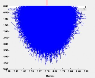
Figure 6. Simulated electron interaction volume at 16 keV for the Hafnia-top sample (145 nm HfO2 on 205 nm SiO2 ). The denser top layer reduces beam spread near the surface, yet the interaction volume still reaches the substrate. High charging risk is present due to HfO2’s poor surface conductivity, despite deeper analytical utility for EDS.
Low-energy scanning electron microscopy (SEM) was performed at 2 keV to examine sur- face morphology of the scratch tracks while minimizing charging effects typically encountered on insulating dielectric materials. The reduced beam energy improved surface sensitivity and contrast, allowing detailed visualization of mechanical deformation features. In the Silica-top sample, the scratch exhibited rough, irregular edges with extensive debris and delaminated fragments distributed along both sides of the trench. The disordered nature of the fracture zone suggests ductile fracture propagation and potential interfacial failure at the SiO2 /HfO2 boundary. In comparison, the Hafnia-top sample displayed a more linear scratch track with sharp-edged tearing and flap-like delamination structures extending laterally. These damage morphologies are indicative of brittle fracture mechanisms characteristic of the top HfO2 layer. Surface texture differences between the two configurations also highlight the influence of top-layer material properties on crack propagation dynamics and stress dissipation during mechanical loading.
A high-magnification SEM image of the HfO2-top sample was acquired at 16 keV to resolve fine-scale morphological features within the scratch zone. The image was subsequently false- color enhanced using a blue-toned overlay to improve visual differentiation of surface structures and fracture planes. The resulting micrograph reveals a complex network of intergranular cracks and angular fracture facets, indicative of brittle mechanical failure. The observed features suggest cleavage-driven propagation and minimal plastic deformation, consistent with the high elastic
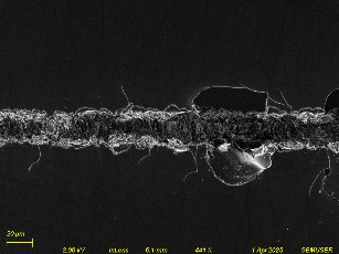
Figure 7. Low-voltage (2 keV) SEM image of the Silica-top sample after nano-scratch testing. The scratch shows a rough and debris-laden morphology with evidence of layer delamination and fracture. Surface damage extends laterally from the trench, suggesting ductile deformation and interfacial failure between the SiO2 and HfO2 layers.
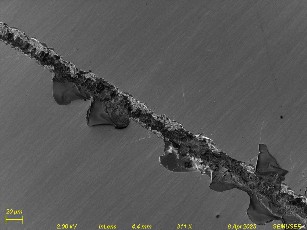
Figure 8. Low-voltage (2 keV) SEM image of the Hafnia-top sample after nano-scratch testing. The scratch track appears more sharply defined, with flap-like material removal indicative of brittle fracture in the top HfO2 layer. Less debris is observed compared to the silica-top configuration.
modulus and low toughness of HfO2. The rough fracture texture and multiple intersecting planes imply heterogeneous stress distribution during loading, leading to catastrophic cracking and material ejection. This high-resolution visualization supports earlier observations from low- voltage SEM and optical microscopy, highlighting the dominant brittle fracture behavior of the HfO2 surface layer under scratch-induced stress.
Energy-dispersive X-ray spectroscopy (EDS) was conducted at 16 keV to characterize ele-
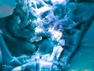
Figure 9. High-resolution, false-color SEM image of the HfO2-top sample showing detailed fracture morphology within the scratch zone. Angular crack networks and cleavage facets dominate the surface, consistent with brittle failure. Blue color enhancement was applied to highlight fracture topography and aid in visual interpretation of microstructural damage.
mental distribution along the scratch paths and to evaluate the extent of material removal in both multilayer configurations. The elevated beam energy was selected to ensure adequate excitation of the Hf Lα and Kα lines, which are critical for resolving HfO2 layers despite their deeper location and higher atomic number. In the Silica-top sample, EDS maps show a strong Si signal in undamaged areas, while the scratch regions exhibit a noticeable decrease in Si and corresponding exposure of underlying Hf and substrate elements, confirming partial or full removal of the silica top layer. Conversely, the Hafnia-top sample shows localized depletion of Hf in the damaged regions, with increasing visibility of Si and substrate-related signals, indicating that the scratch force penetrated through the HfO2 layer into the SiO2 and possibly to the fused silica base. These results are consistent with the mechanical observations and provide compositional confirmation of sequential layer failure and material ejection during nano-scratch testing.
Atomic force microscopy (AFM) was employed to evaluate the initial surface roughness and to- pographic uniformity of the as-deposited thin films in non-scratched regions. These measurements establish baseline conditions for assessing damage-induced changes and ensure that pre-existing roughness or particulates did not influence scratch propagation behavior. The Silica-top sample exhibited a smooth, undulating surface with a peak-to-valley height variation of approximately 16 nm over a 1 µm×1 µm scan area, consistent with typical SiO2 film deposition characteristics. In contrast, the Hafnia-top sample demonstrated a higher degree of vertical roughness, reaching
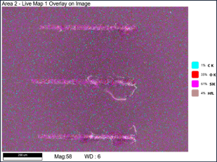
Figure 10. EDS elemental overlay map of the Silica-top sample at 16 keV. The scratch regions show reduced Si (blue) and enhanced signals of Hf (pink) and substrate-associated elements, indicating abrasion through the SiO2 top layer and partial exposure of the underlying HfO2.
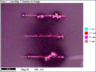
Figure 11. EDS elemental overlay map of the Hafnia-top sample at 16 keV. Scratched areas show reduced Hf (pink) and enhanced Si (orange), suggesting complete removal of the top HfO2 layer and partial penetration into the SiO2 layer below.
up to 45 nm peak features across a broader 5 µm × 3.9 µm scan area. However, this AFM data was selectively cropped to exclude micron-scale particulate contaminants, which may have resulted from post-deposition handling or airborne contamination. The preserved topographic detail confirms a rougher intrinsic surface morphology for HfO2 relative to SiO2 , which may contribute to differential adhesion, fracture initiation, and charging behavior observed in SEM and EDS analyses.
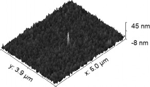
Figure 12. AFM surface topography of the Silica-top sample over a 1 µm × 1 µm region. The smooth, periodic undulations and low vertical roughness confirm uniform surface quality in non-damaged regions.
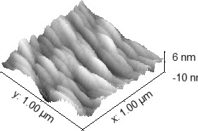
Figure 13. AFM surface topography of the Hafnia-top sample, cropped to remove particulate contamination. The higher roughness (up to 45 nm) and irregular morphology reflect the intrinsic surface characteristics of the HfO2 layer.
IV. Discussion
The combination of nano-scratch testing and high-resolution characterization provided detailed insights into how layer composition and sequence affect damage propagation in multilayer dielectric stacks. Optical microscopy (DIC mode) revealed distinct failure morphologies for each sample. The SiO2 -top sample exhibited diffuse delamination and interference patterns, indicative of stress localization and potential interfacial shearing. The HfO2-top sample showed wider, more sharply defined scratch zones with lateral cracking, suggesting brittle top-layer failure. Low-voltage SEM imaging at 2 keV provided surface-sensitive morphological contrast without inducing excessive charging. The SiO2 -top sample exhibited widespread debris and irregular trench morphology, while the HfO2-top sample showed cleaner trench formation but
pronounced flap-like delamination. High-resolution, false-color SEM of the HfO2-top sample further confirmed angular cleavage and fracture facets consistent with brittle failure mechanisms. EDS mapping at 16 keV demonstrated material-specific ablation and provided compositional verification of layer removal. In both cases, scratches extended beyond the top layer, exposing the underlying dielectric and, in some instances, the fused silica substrate. This was validated by elemental depletion zones and redistributed signal intensity in the Hf and Si maps. Elec- tron interaction simulations supported these findings by showing that 16 keV electrons readily penetrated through both dielectric layers into the substrate, confirming the risk of charging during imaging but validating beam energy requirements for EDS analysis. AFM scans in non- scratched regions provided baseline surface morphology. The SiO2 surface was smoother, with nm-scale undulations, while the HfO2 surface showed higher roughness even after cropping to exclude particulates. These roughness differences likely influence initial crack formation, interfacial adhesion, and charge dissipation during SEM. Together, these techniques revealed that although both configurations undergo full layer removal under scratch loading, the HfO2- top sample is more prone to brittle fracture and charging effects, while the SiO2 -top sample demonstrates more ductile deformation and interfacial instability. The results suggest that layer sequence and top-layer material selection are critical factors in tailoring mechanical durability in dielectric film stacks.
V. Conclusion
This study systematically evaluated the mechanical failure and surface response of two multi- layer dielectric film configurations using nano-scratch testing and comprehensive characterization methods. The HfO2-top stack demonstrated increased brittleness, higher roughness, and greater charging susceptibility, leading to flap-like delamination and brittle fracture. The SiO2 -top stack, while also undergoing full ablation under sufficient load, exhibited more ductile damage propagation and interfacial delamination. SEM and EDS confirmed material removal patterns and validated simulation-based predictions of electron beam penetration depth. AFM further emphasized the difference in intrinsic surface morphology between the two top layers. These findings underline the importance of material selection and layer sequencing in engineering multilayer films for applications demanding mechanical robustness and surface resilience.
Acknowledgment
I would like to thank D. Broege from the Laboratory for Laser Energetics (LLE) and J.C. Lambropoulos from the University of Rochester for providing these samples for analysis as well as S. O’Neill for characterization assistance.