University of Rochester, Materials Science Program
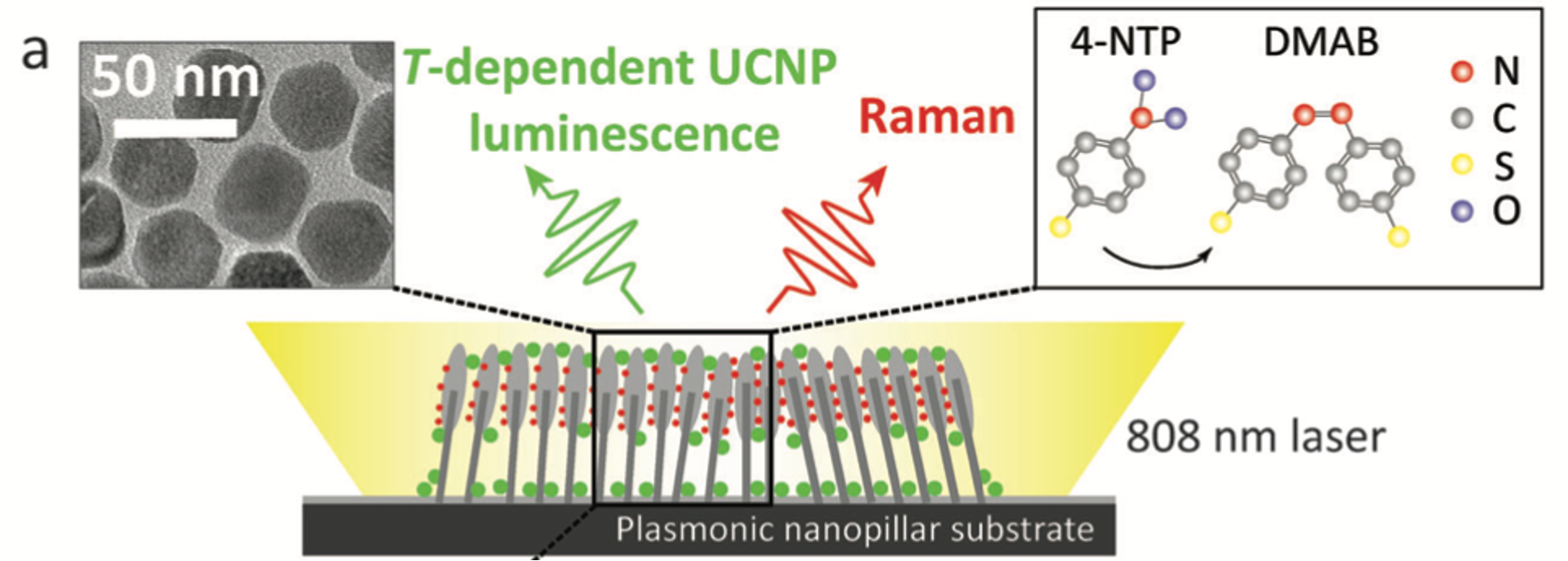
As shown in fig 1, in our lab, we are trying to decouple laser intensity effects from photothermal heating in the photocatalysis. When plasmonic nanoparticles or structures are exposed to light, their conduction electrons oscillate collectively, creating a resonant condition called Localized Surface Plasmon Resonance (LSPR), and the surface plasmon resonance happens when the frequency of the incident light matches the natural frequency of these electron oscillations. Once these plasmons are excited, they will decay and transfer their energy to the electrons. That decay process generates hot electrons. These hot electrons have energies above the Fermi level and are energetic enough to jump into nearby molecules and participate directly in chemical reactions. They might break molecular bonds, or initiate charge transfer, making reactions go faster or happen at lower energy. However, these hot electrons quickly undergo electron-electron scattering, followed by electron-phonon interactions, which transfer energy to the lattice and increase the local temperature. Thus, a portion of plasmon energy is converted into heat, which further contributes to catalysis by reducing activation energy barriers. The extent of this temperature rise depends on the optical absorption, geometry, and thermal dissipation properties of the plasmonic nanostructures and their substrates. The extent of temperature rise resulting from this process is governed not only by the optical absorption properties of the plasmonic nanostructure but also by its thermal dissipation efficiency, which is dictated by the nanostructure geometry and the thermal conductivity of the underlying substrate. To decouple laser intensity effects from photothermal heating, we aim to maintain a constant laser intensity while selectively modifying the thermal dissipation properties of the system through nanostructural variations. In that way we need to make our own plasmonic structure: Ag and Au nanoislands. And use ucnps to measure the temperature change.
Fig. 1. Schematic showing the T-dependent UCNP luminescence and Raman process on a plasmonic nanopillar substrate under 808 nm laser excitation. Insets show TEM image and molecular conversion from 4-NTP to DMAB.
The goal of this project was to characterize our gold and silver nanoislands used in plasmonic photocatalysis using AFM, SEM, EDX and imagej analysis, and also characterize the ucnps used as upconversion luminescence thermometry using TEM and ImageJ analysis.
A non-contact mode was used in AFM imaging, as shown in figure 2, the gold nanoislands has higher height because they are underdoing higher temperature and time for annealing, and silver nanoislands has lower height and size because they are undergoing lower temperature and time for annealing. Which is correspond to the sem images shown below.
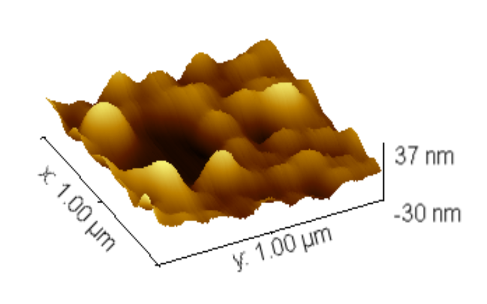
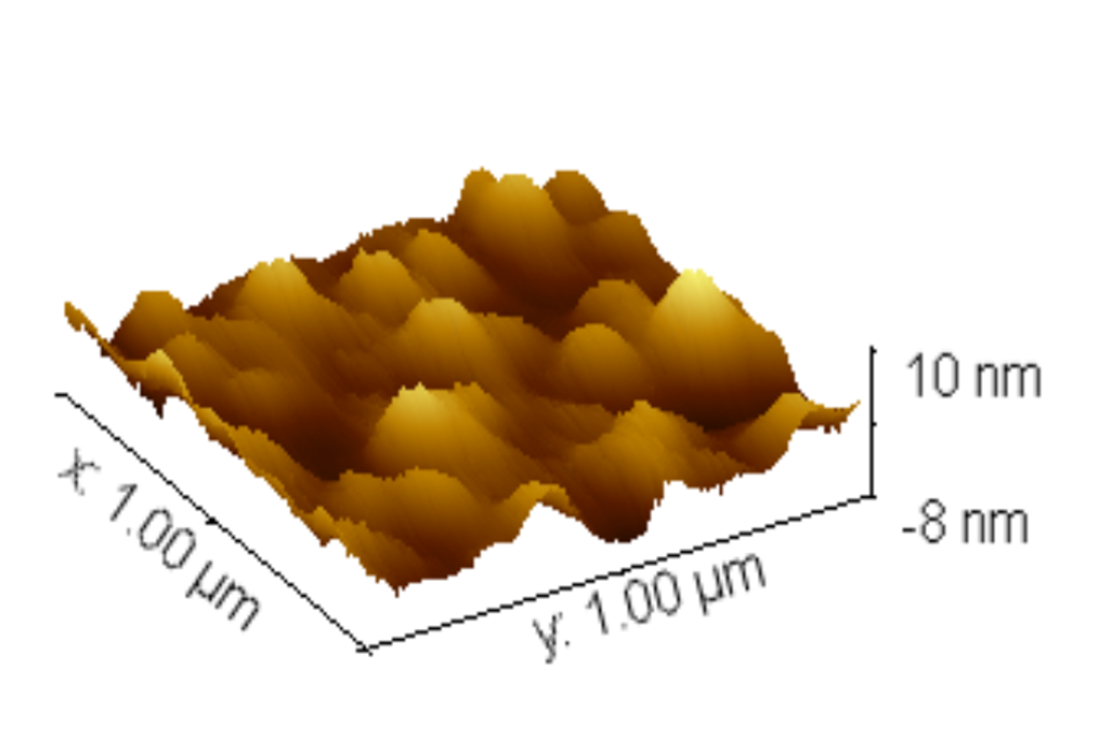
Fig. 2. AFM images for Au nanoisland with 65s Pt coating(left) and Ag nanoislands with 65s Au coating (right)
Before the sem imaging, we need to coat our sample to be conductive and reduce charging effects, because our sample’s substrate is nonconductive glass. A 65s pt coating was sputtered to form an appropriately 60A pt thin film on the sample. Also to further reduce the charging effect, an additional copper tape is used to connect the sample and the sample mount. As shown in fig 3, the images are taken using the inlens detector using 7 kv accelxerating voltage under low working distance 5 mm to achieve best resolution. Inlens detector detects the secondary electrons and short working distance enhance the electron signals in the inlens detector and could also increase the resolution by reducing the spot size. The low accelerating voltage are used because our sample’s height is small, and we need more signal from the surface topography. Imagej was used to characterize the islands area size. For gold nanoislands, which are widely separated and have high contrast, the same process as we did in lab was used to analyze their size: subtract background, enhance contrast, the threshold image, despeckle, and watershed to ungroup multiple particles. For silver nanoislands, because the image contrast is too low and the islands are too densely packed and are attached to each other, it’s hard to subtract them using threshold. So their sizes are measured manually. By analyzing the images using imagej as shown in fig 4, and convert the pixels to nm using scale bar, the results reported that:
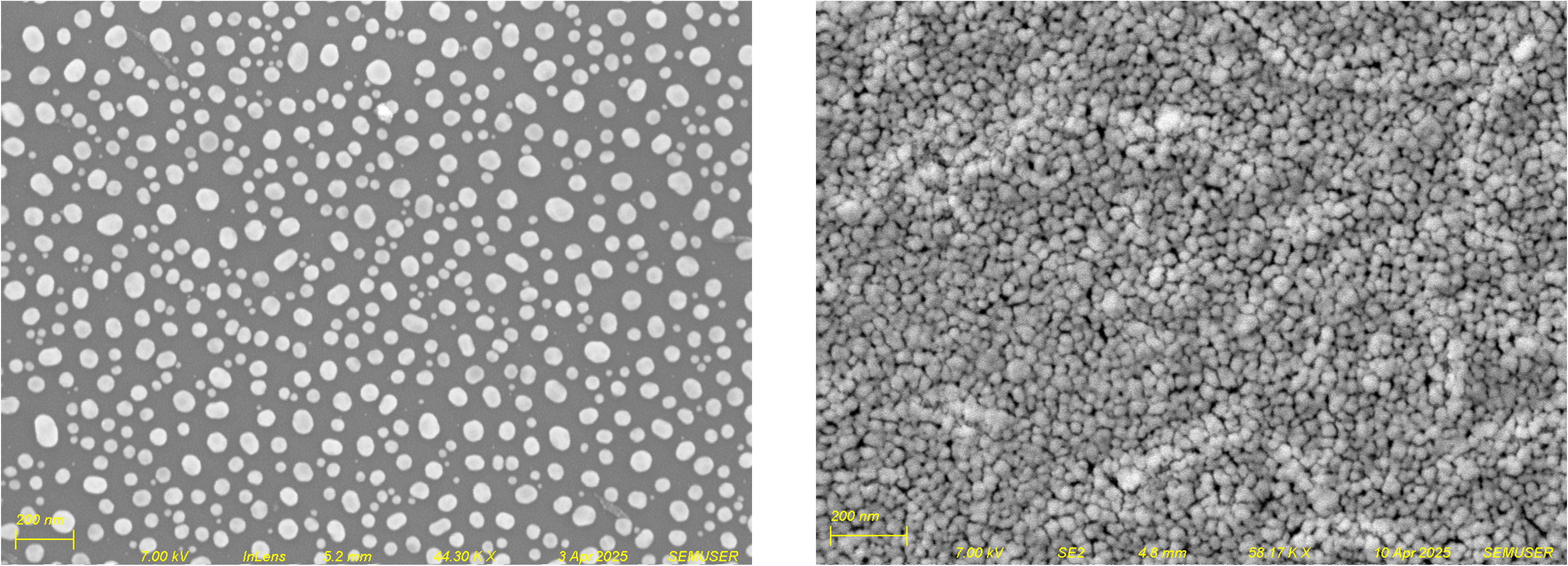
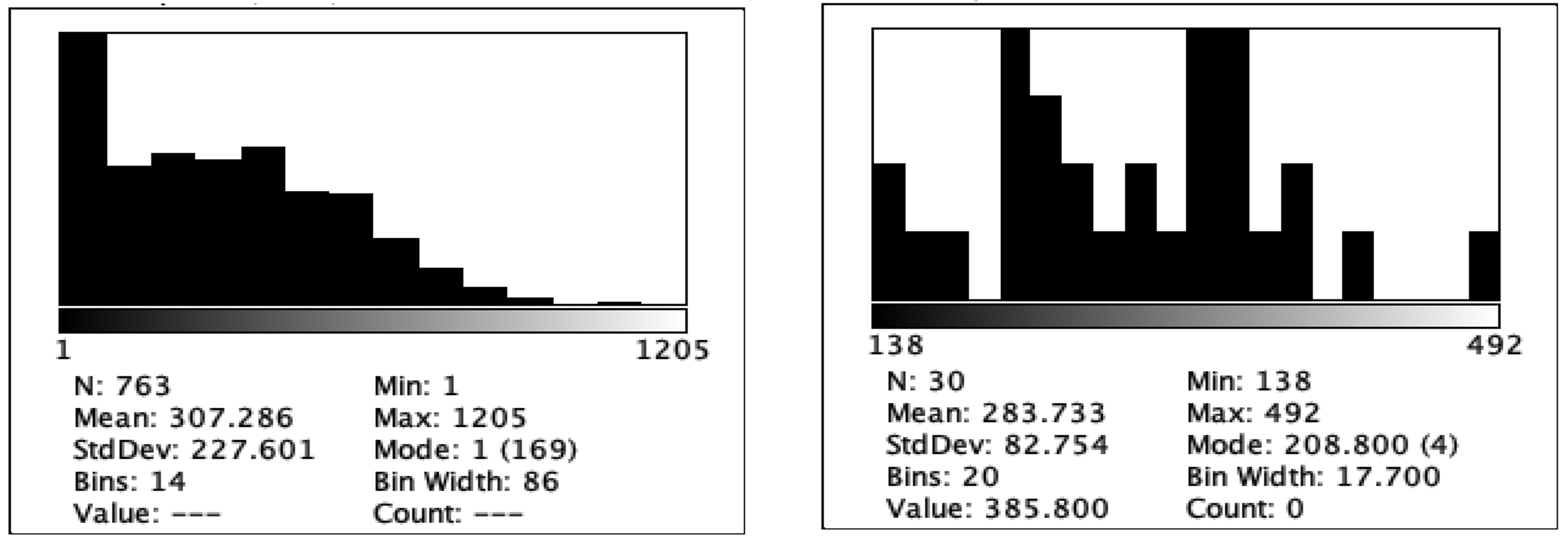
Fig. 4. Area distributions in pixels for Au nanoisland with 65s Pt coating(left) and Ag nanoislands with 65s Au coating (right)
From the results of EDX spectrum of NIs shown in figure 5, it is clearly to see the Au and Ag signals, just to make sure the fabrication is correct.
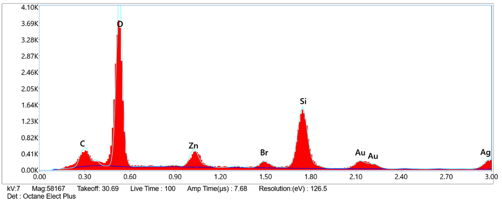
Fig. 5. Elemental spectrum for Ag nanoislands with 65s Au coating
The Upconverting nanoparticles (UCNPs): NaYF4 co-doped with Yb3+ (20 at.%), and Er3+ (2 at.%) were purchased from a commercial supplier that claims a uniform size distribution. Since the size of the UCNPs significantly impacts the experimental results of the lab analysis it was important to verify that the manufacturer's specifications were accurate before any UCNPs were being utilized in lab experiments. UCNPs were dispersed along a TEM carbon support mesh. As shown in fig 6, TEM images were taken under bright field imaging conditions. To maximize the image contrast, the image was set to be slightly underfocused. By analyzing the images using ImageJ, the results shown in fig 7 reported that:
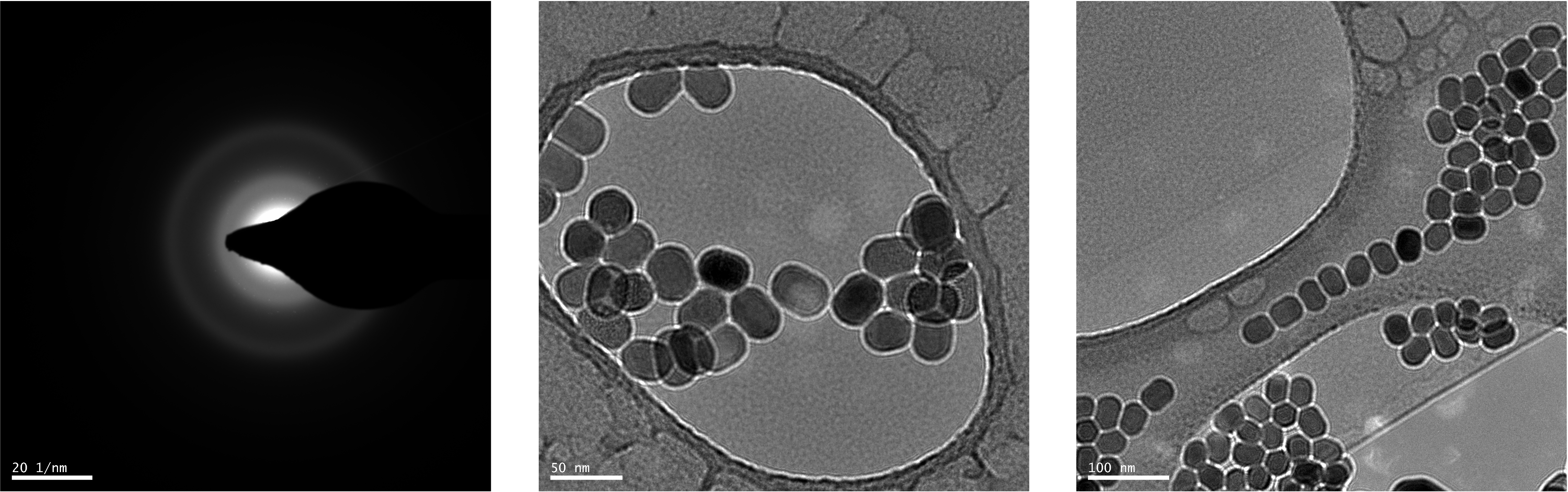
Fig. 6. Diffraction rings and TEM images for upconversion nanoparticles (UCNPs):NaYF4 UCNPs co-doped with Nd3+ (0.5 at.%), Yb3+ (20 at.%), and Er3+ (2 at.%)
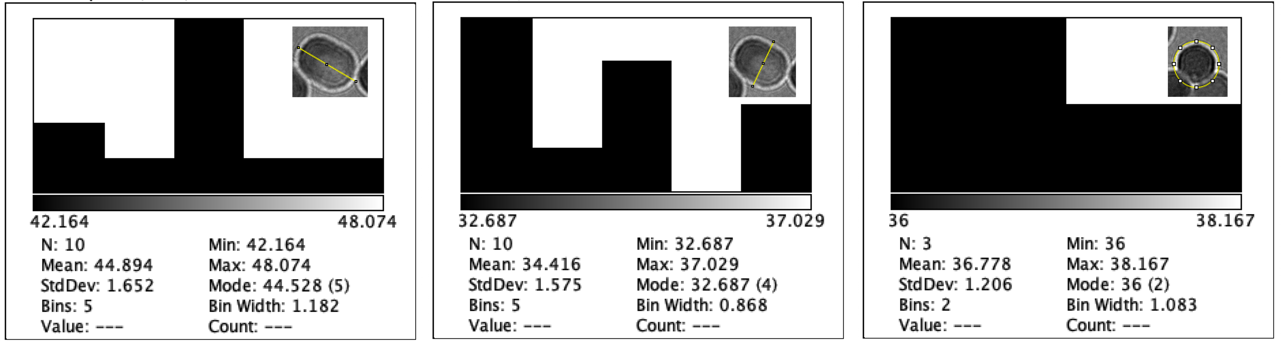
Fig. 7. Area distributions in nm^2 for upconversion nanoparticles (UCNPs) length, height, circular radius
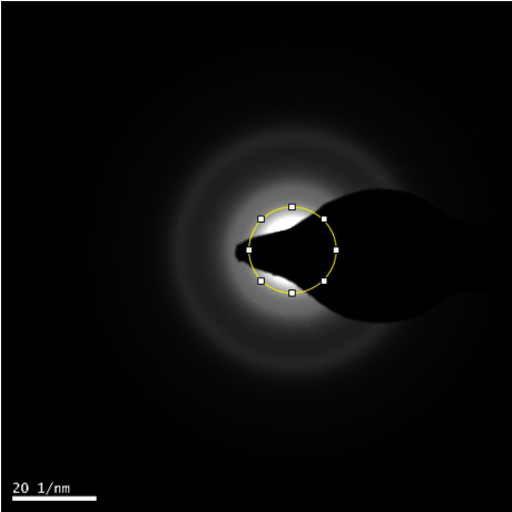
Fig. 8. Diffusion rings for UCNPs
Gold and silver nanoislands were successfully fabricated and characterized. UCNPs size and crystallinity were confirmed. The average nanoislands size for gold is 2026.04 nm^2, and for silver is 1069.78 nm^2. The gold NIs are more widely spaced, whereas the silver NIs are densely packed together. From the EDX spectrum of NIs, we could clearly see the Au and Ag signals. Size characterization of our UCNPs: average length = 44.89 nm; average height = 34.42 nm; average circular diameter = 36.78 nm. Based on the diffraction image, the {111} interplanar spacing of UCNPs is 3.3A, which is similar to the data in the literature.
Thanks to Laura Kowalski, Ben Harrington, and Sean O’Neill for assistance. Acknowledgment to the Nanoscale Thermal Transport Lab and Professor Andrea Pickel for support and resources.
© 2025 UCNP Photocatalysis Project