Introduction
While photolithography, electron beam lithography, and focused ion beam milling remain the conventional standards for nanofabrication, femtosecond (fs) direct laser processing has emerged as a compelling alternative. It offers several distinct advantage [1]. It enables maskless, resist-free patterning of multiscale structures, maintains the versatility to process non-planar surfaces across nearly all materials and bypasses the stringent requirement for cleanroom environments [1]. However, the widespread utility of fs-laser processing is often hindered by the inherent stochastic nature of ultrafast laser-matter interactions, which can result in irregular, poorly reproducible nanostructures.
To address these limitations, our group recently developed a new technique to produce highly periodic nanobumps on glass using a sacrificial plasmonic layer [1]. While effective, the introduction of this intermediary layer adds a new layer of complexity to the interaction, as the energy transfer is no longer directly into the material of interest. For this technique to mature into a reliable nanofabrication standard, it should be controllable and reproducable. This can only be achieved through a thorough understanding of the formation dynamics.
The objective of this semester project is to try and understand the underlying physics. This will be achieved by characterizing not only the final morphologies but also the intermediary nano-structures formed during irradiation, which might hold clues on the governing physical mechanisms.
Theory
The interaction between fs lasers and condensed matter is fundamentally defined by the different timescales at which electronic excitation and lattice heating take place [2]. Unlike lasers with longer pulse durations (nanosecond or longer), where thermal diffusion dominates, a fs pulse deposits energy into the electronic system much faster than the time available for the said electrons to transfer this energy to the lattice through phonon scattering (Fig. 1.1) [2]. This results in a state of strong thermodynamic non-equilibrium and heat localization, allowing for material removal with a negligible heat affected zone [2].
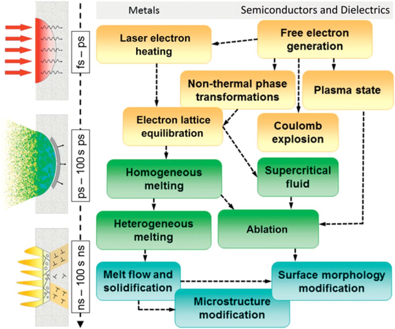 Fig. 1.1
Timescales of physical processes induced by a fs laser pulse in
metals, dielectrics, and semiconductors [2].
Fig. 1.1
Timescales of physical processes induced by a fs laser pulse in
metals, dielectrics, and semiconductors [2]. In metals, incident laser energy is absorbed by the dense sea of conduction band electrons via inverse Bremsstrahlung [3]. This process is traditionally described by the Two-Temperature Model (TTM) [3,4], which tracks the evolution of the electron temperature and the lattice temperature as two coupled subsystems. In contrast, dielectrics and semiconductors lack these initial free electrons, making them transparent to low intensity light. Interaction here relies on nonlinear absorption mechanisms like Multiphoton Ionization to bridge the wide bandgap and generate free electrons [5].
Sample Fabrication
Substrates consisting of 1 mm thick microscope slides and quartz wafers were cleaned via sequential rinsing with acetone and isopropyl alcohol. The samples were immediately dried under compressed nitrogen gas and dehydrated on a hotplate at 40°C for 15 minutes. Finally, a 100 nm Cu film was deposited using the KLJ PVD-75 thin-film deposition tool at the URNano cleanroom facility.
Irradiation experiments were performed using an amplified Ti:Sapphire laser (1 kHz repetition rate, 800 nm wavelength, 65 fs pulse duration). Laser power was regulated using a half-wave plate and a polarizing beamsplitter cube, followed by a quarter-wave plate set at 45° to generate circularly polarized light. A mechanical shutter with a 1 ms response time was used to isolate single pulses at a time. The beam was focused through a 50 mm plano-convex lens onto the sample, which was mounted on an XYZ translation stage. For all trials, a power of 115 mW was applied with the sample positioned approximately 2 mm above the focal plane. In some specific trials, a circular aperture was introduced into the beam path to induce diffraction which served to enhance the visibility of the resulting nano-structures. The optical setup is shown in Fig. 2.1.
As the goal of this project is to understand the formation mechanism by mapping the intermediary nano-structures formed, an irradiation matrix was generated. A gradient of incident pulses ranging from 1000 to 40000 was applied across spatially seperated regions of the sample to ensure that each spot represents a distinct stage of the structural evolution.
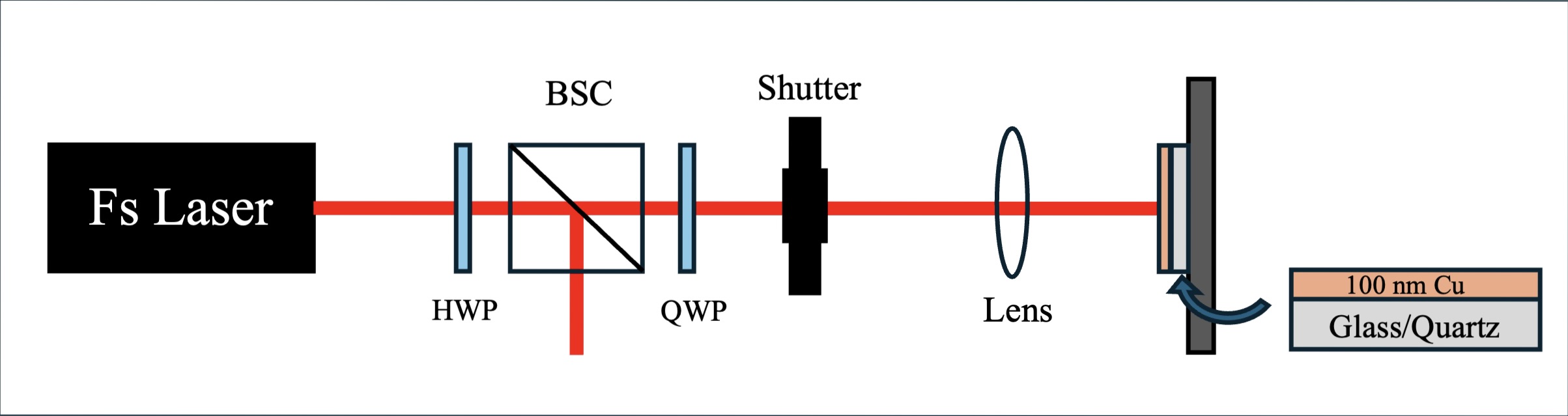 Fig. 2.1
Schematic of the optical setup for pulse-by-pulse sample
irradiation.
Fig. 2.1
Schematic of the optical setup for pulse-by-pulse sample
irradiation. Sample Characterization
Light Microscopy
The Olympus BX51 Light Microscope available at URNano was used throughout the experiements to determine the spot size of the focused beam and for studying the effect of the pinhole aperture in generating a diffracted beam. Most of the viewing and imaging was done in Differential Interference Contrast (DIC) mode at 50x magnification as the pseudo-3D images produced allowed us to determine whether 2D nanostructures were even present on the substrate surface before taking SEM images.
Scanning Electron Microscope
The primary metrology tool used in this study was the Zeiss Auriga SEM available at URNano. Since the nano-structures of interest were formed on glass and quartz, all the samples were sputter coated with ~ 10 nm Pt layer via the Dento Vacuum DESK-II DC Sputtering System and grounded via conducting tape. In order to maximize resolution, the SEM's InLens detector was used for secondary electron imaging along with shorter working distances ranging from ~ 2.2 to 5.2 mm. In this study, primarily 5 and 20 kV accelerating volatages were used. 5 kV was used to get the fine surface details while 20 kV was used for higher resolution imaging of the intermediate nano-particles.
Energy Dispersive Spectroscopy
While taking SEM images, the built in EDAX X-ray Spectrometer was commonly used to determine wether the structures being imaged were from the Cu film or the substrate itself. EDS was typically done at 20 kV accelerating voltage to ensure signal from all the expected elements and to ensure a sufficient number of counts. EDS mapping was done for ~ 20 mins in order to get enough resolution for the elemental map.
Atomic Force Miscroscopy
Once periodic nano-strucutres were succesfully generated and imaged via the SEM, the NTMDT AFM Microscope available at URNano was used to generate 3D topographical maps of the structures to determine height and periodicity. All AFM scans were done using the semi-contact mode on the device.
Results and Analysis
Diffracted vs Un-Diffracted Beam
The Airy disk pattern generated in the incident beam when an aperture is placed in the optical beam path results in alternating rings where ablation occurs and where it doesn't. DIC images of the diffracted and un-diffracted spots are shown in Fig. 3.1 and 3.2 respectively. Interestingly, the DIC alone is capable of highlighting where nano-strucutres may be present as it translates minute variations in the samples surface gradient and optical path length into intensity contrast.
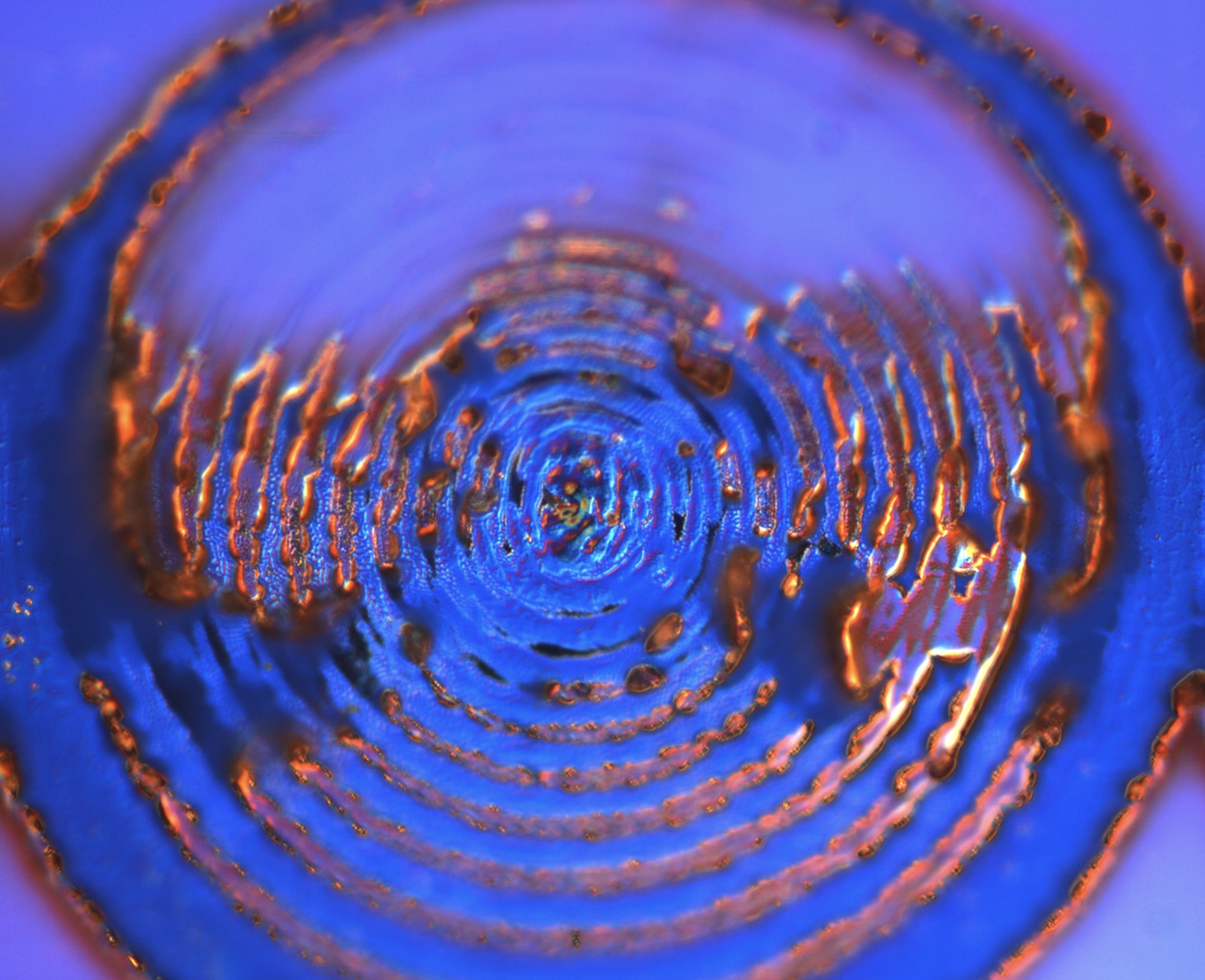 Fig.
3.1 Spot with the aperture
showing the diffraction pattern. 50x magnification.
Fig.
3.1 Spot with the aperture
showing the diffraction pattern. 50x magnification. 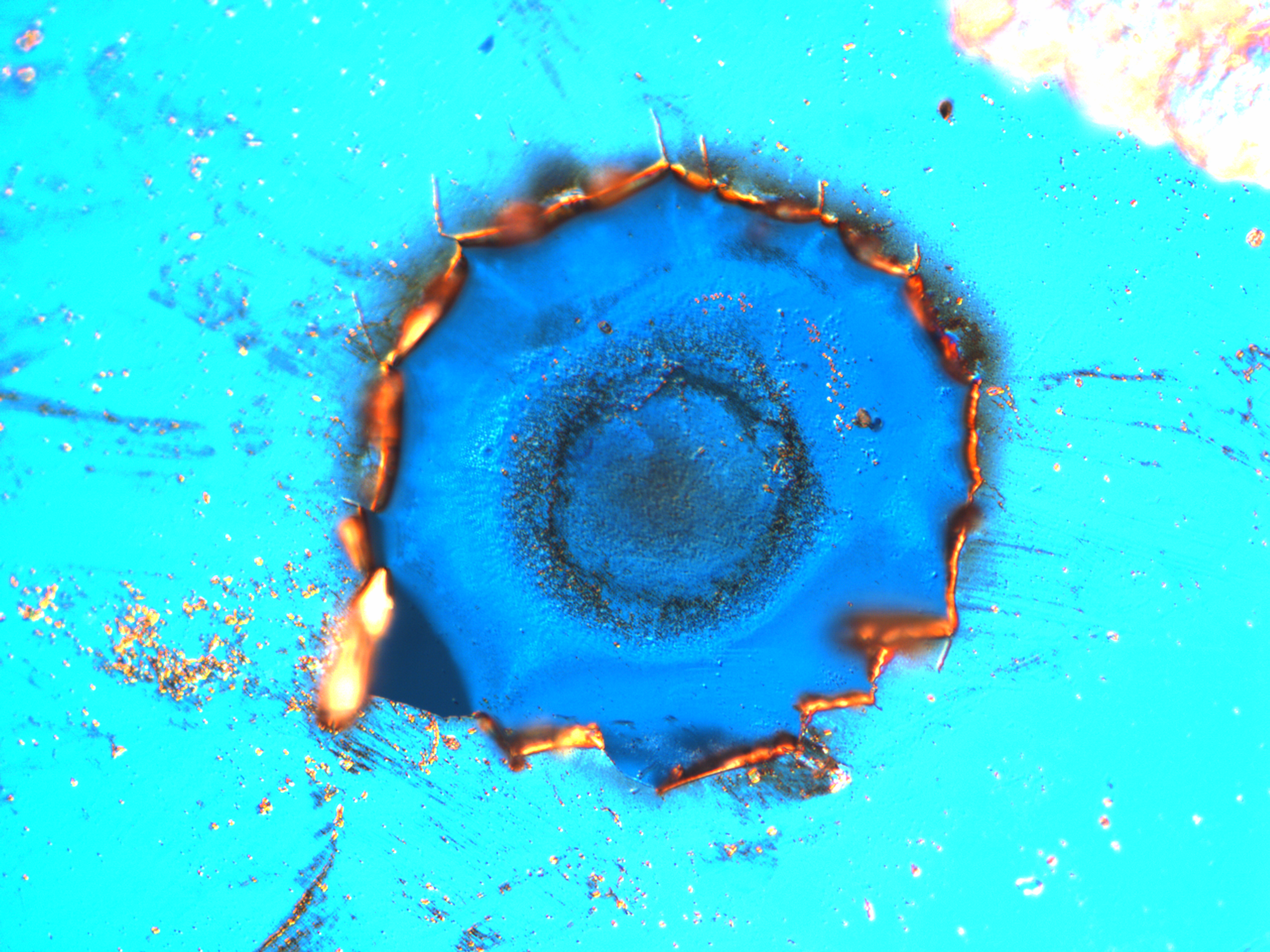 Fig.
3.2 Spot without the
aperture. 50x magnification.
Fig.
3.2 Spot without the
aperture. 50x magnification. Spatial Distribution of Nano-structures
Due to the Gaussian nature of the incident beam, the energy density decreases radially from the beam's center to its edge. As a result, a single laser spot acts as a microcosm of structural evolution, hosting a wide range of nano-structures simultaneously. This is clearly seen in Fig. 4.1.
 Fig. 4.1 SEM
images depicting the variety of nano-structures generated along with
their hierarchical nature.
Fig. 4.1 SEM
images depicting the variety of nano-structures generated along with
their hierarchical nature. Evolution of Nano-structures for Quartz without Aperture
The systematic evolution of surface nano-structures was studied as a function of the number of incident pulses. As the number of incident pulses increases, the surface undergoes a distinct morphological transition, evolving from initial randomized pitting to self-organized periodic features. As mentioned earlier, the Gaussian distribution of the laser spot results in a spectrum of features that varies spatially. Therefore, to provide a standardized timeline of this evolution, SEM micrographs were taken from the same relative position within the spot for each sample, ensuring that the observed structural changes are strictly a result of the pulse count rather than fluence variations within the spot.
The transition from a continuous Cu film to complex substrate nano-structures is a multi-step process that can be described as follows. Firstly, the initial 1000 pulses deliver enough thermal energy to the Cu film to exceed its stability threshold. This causes the film to fracture into isolated fragments and particulates. Within the subsequent 1000 pulses, the system undergoes liquid state dewetting. To minimize total surface free energy, the molten Cu remnants retract from the substrate and self-organize into nanoparticles.
Once the Cu nano-particles are formed, they serve as optical antennas that trigger Localized Surface Plasmon Resonances (LSPR) [1]. This effect strongly confines and enhances the electromagnetic field at the nanoparticle-substrate interface. The resulting near-field intensity far exceeds the average intensity of the beam itself, causing localized melting or ablation of the underlying susbtrate at these hot spots. This targeted energy deposition results in the formation of discrete nano-bumps directly beneath the metal particles.
Finally, as the irradiation continues, the density of these nano-structures increases. The cumulative thermal load applied along with the expansion of the localized plasmonic hot spots cause the individual nano-bumps to interfere with one another. Eventually, these features merge to form self-organized nano-ridges that are typically known as Laser Induced Periodic Surface Structures (LIPSS).
 Fig. 6.1 1000
Pulses.
Fig. 6.1 1000
Pulses.  Fig. 6.2 2000
Pulses.
Fig. 6.2 2000
Pulses.  Fig. 6.3 3000
Pulses.
Fig. 6.3 3000
Pulses.  Fig. 6.4 6000
Pulses.
Fig. 6.4 6000
Pulses. 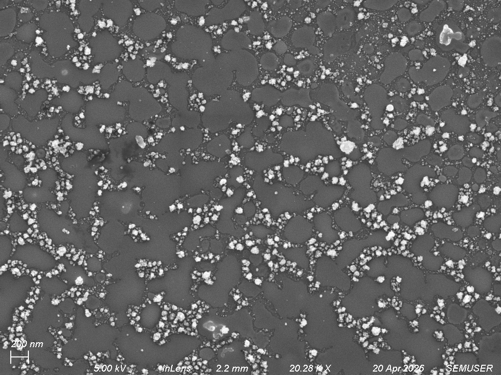 Fig. 6.5 10000
Pulses.
Fig. 6.5 10000
Pulses. Evolution of Nano-structures for Glass with Aperture
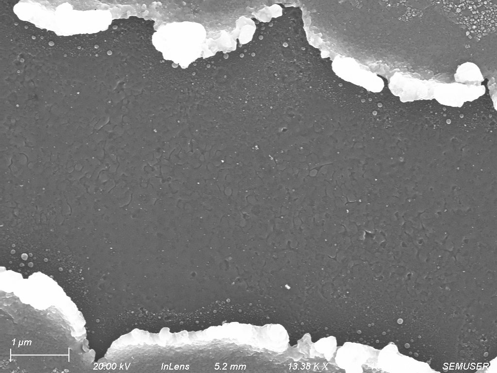 Fig. 7.1 1000
Pulses.
Fig. 7.1 1000
Pulses.  Fig. 7.2 2000
Pulses.
Fig. 7.2 2000
Pulses. 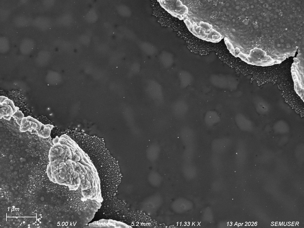 Fig. 7.3 8000
Pulses.
Fig. 7.3 8000
Pulses. 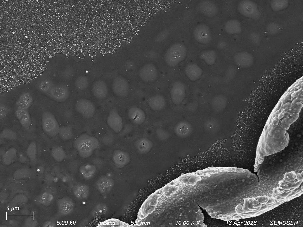 Fig. 7.4 22000
Pulses.
Fig. 7.4 22000
Pulses. 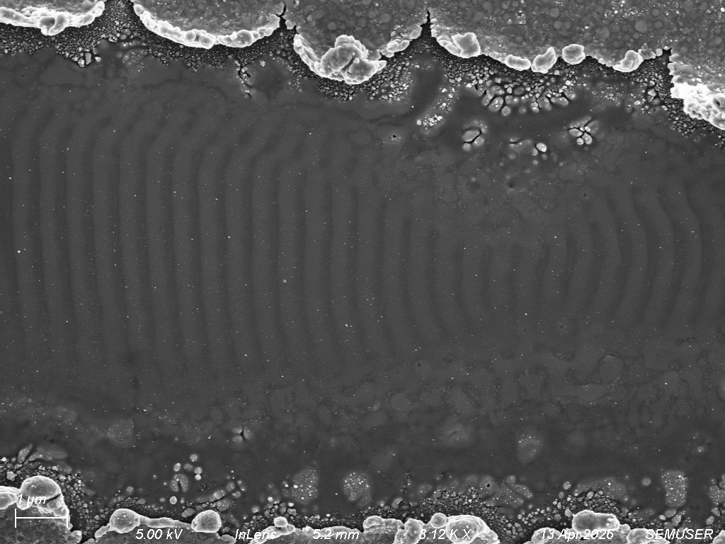 Fig. 7.5 32000
Pulses.
Fig. 7.5 32000
Pulses. AFM Analysis
AFM was also conducted on the primary structures of interest to create 3D topographical maps. After the data was collected, background correction and periodicity and height analysis was done using Gwyddion. The results for the generated LIPSS are presented in Fig. 8.1, 8.2, 8.3 while the results for the generated nano-bumps are presented in Fig. 8.4, 8.5, 8.6. The white lines overlayed in Fig. 8.2 and 8.5 indicate where the 1D profiles in Fig. 8.3 and 8.6 are obtained from. For the LIPSS, the periodicity is ~ 535 nm while the height is ~ 22 nm. For the nano-bumps, the periodicity is ~ 850 nm while the height is ~ 69.8 nm.
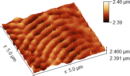 Fig.
8.1 3D AFM scan of the
generated LIPSS.
Fig.
8.1 3D AFM scan of the
generated LIPSS. 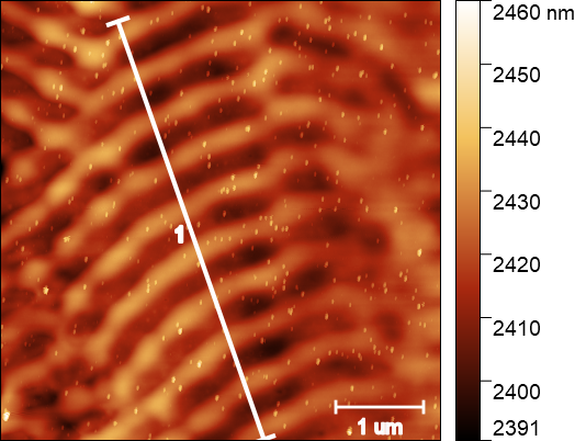 Fig.
8.2 2D AFM scan of the
generated LIPSS.
Fig.
8.2 2D AFM scan of the
generated LIPSS. 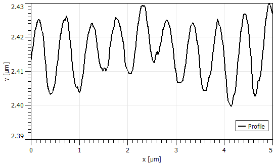 Fig.
8.3 1D profile of the
generated LIPSS.
Fig.
8.3 1D profile of the
generated LIPSS. 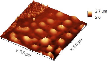 Fig.
8.4 3D AFM scan of the
generated nano-bumps.
Fig.
8.4 3D AFM scan of the
generated nano-bumps. 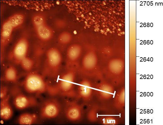 Fig.
8.5 2D AFM scan of the
generated nano-bumps.
Fig.
8.5 2D AFM scan of the
generated nano-bumps. 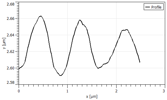 Fig. 8.6 1D
profile of the generated nano-bumps.
Fig. 8.6 1D
profile of the generated nano-bumps. EDS Analysis
To ensure that the Cu film is completely ablated away, resulting in nano-structures on the substrate alone, EDS was conducted. It should be noted that the utility of the diffracted beam in analysis is most prominent here. The variations in the intensity of the beam resulted in a contrast map of where the Cu film remains and where it is ablated away allowing for a sharper distinction between the generated structures and the underlying substrate. The results of the EDS analysis is presented in Fig. 9. Fig. 9.1 and 9.2 show the original SEM image and the overlayed elemental maps respectively. Fig. 9.4, 9.5 and 9.6 clearly show that the structures are generated in the trench between the Cu film on the glass susbtrate.
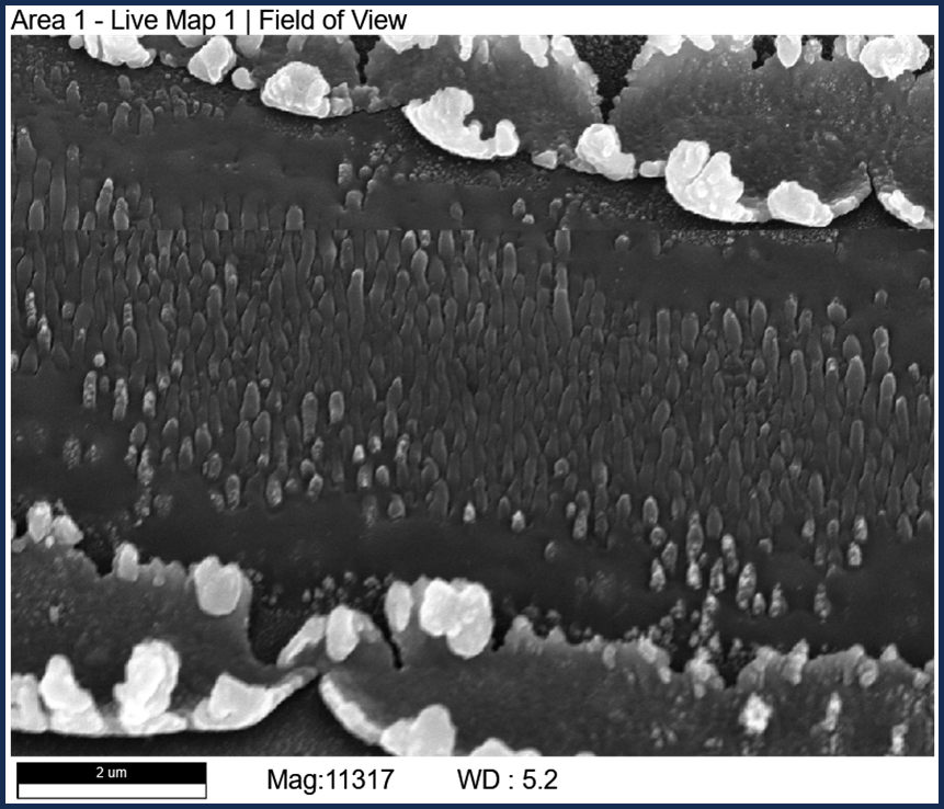 Fig.
9.1 SEM of the glass sample.
Fig.
9.1 SEM of the glass sample.
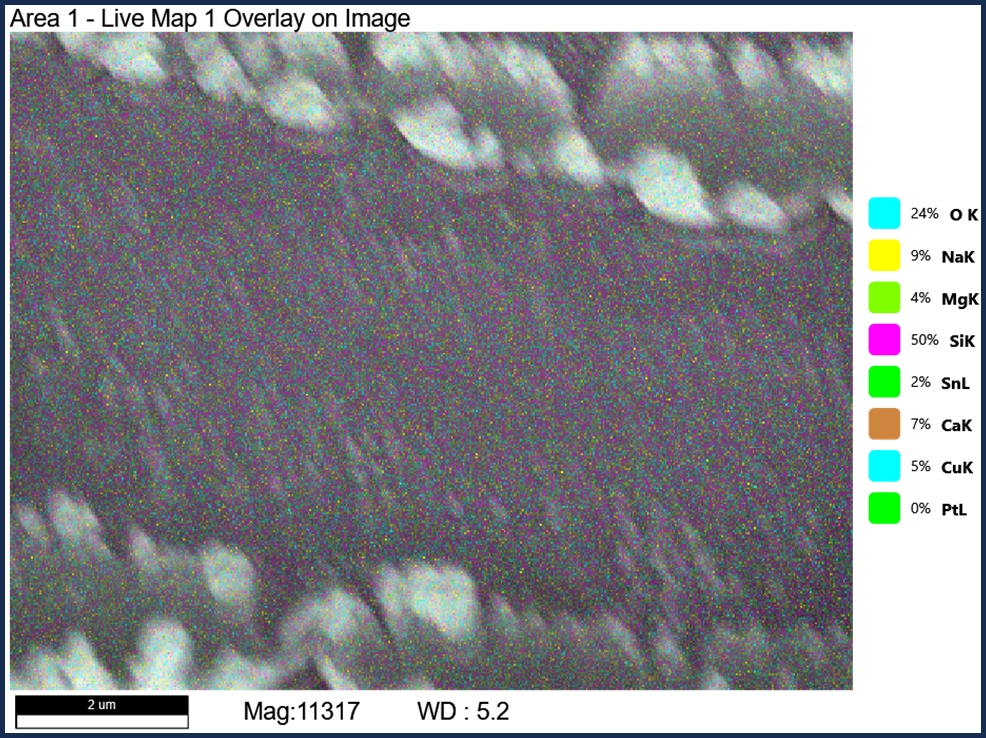 Fig.
9.2 Overlayed EDS elemental
map of the glass sample.
Fig.
9.2 Overlayed EDS elemental
map of the glass sample. 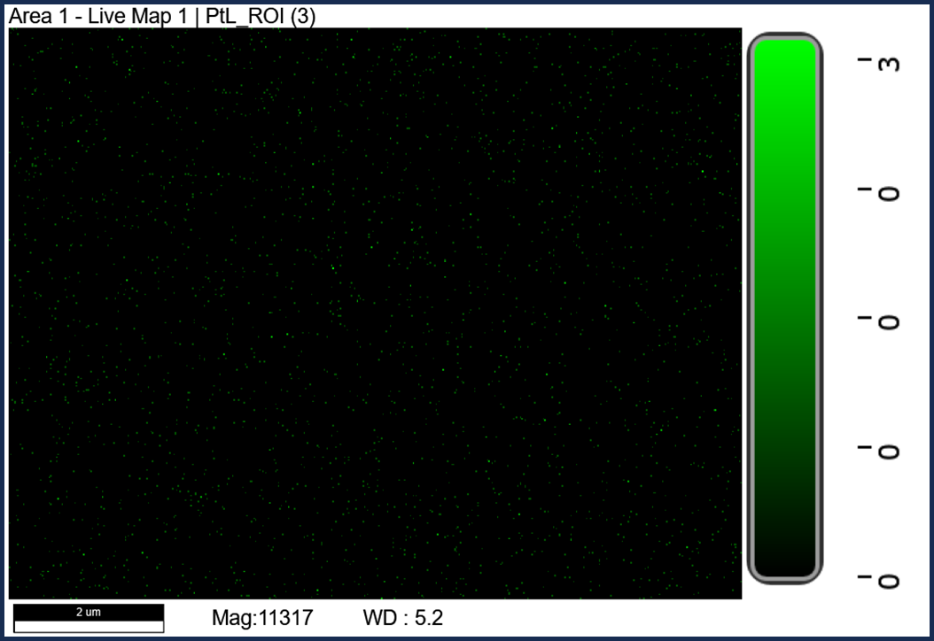 Fig.
9.3 Pt elemental map for the
glass sample.
Fig.
9.3 Pt elemental map for the
glass sample. 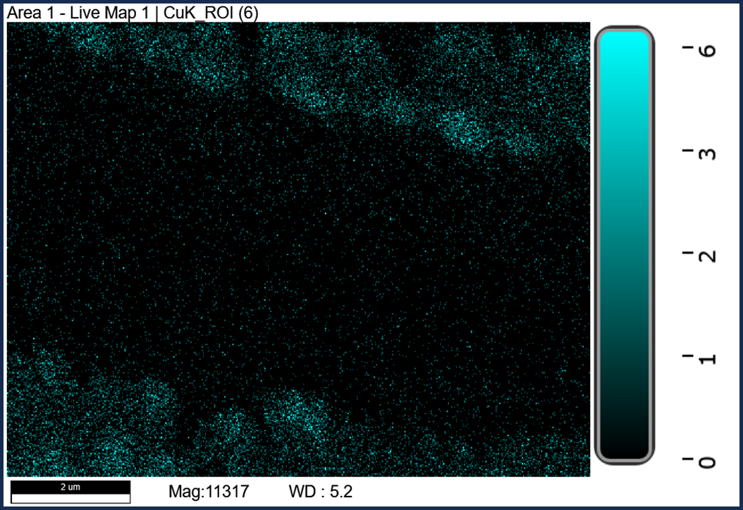 Fig.
9.4 Cu elemental map for the
glass sample.
Fig.
9.4 Cu elemental map for the
glass sample. 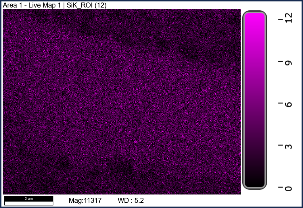 Fig.
9.5 Si elemental map for the
glass sample.
Fig.
9.5 Si elemental map for the
glass sample. 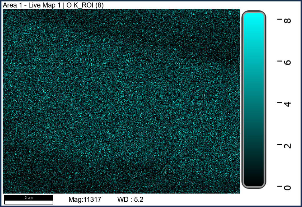 Fig. 9.6 O
elemental map for the glass sample.
Fig. 9.6 O
elemental map for the glass sample. 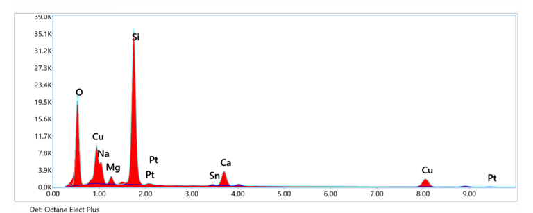 Fig. 9.7 EDS
spectrum for the glass sample.
Fig. 9.7 EDS
spectrum for the glass sample. Tilt Sequence and Anaglyphs
When studying the multitude of nano-structures generated, localized formations of 'nano-needles' were observed at specific regions of the diffracted glass sample. These high-aspect-ratio structures are of particular interest due to their versatile functional applications. To clearly visualize the vertical growth and the extrusion of these needles from the substrate surface, a tilt sequence was performed using the SEM. This was done by first making sure the sample is at the precise eucentric height in order to prevent the region of interest from shifting off-center during the tilt. A tilt sequence from 0° to 40° was then conducted with 5° increments. Afterwards, the image processing software Fiji was used to align the images in the stack and generate anaglpyh pairs. Anaglyph pairs were generated as they provide a pseudo-3D representation of the topography of the 'nano-needles'. An SEM image of the sample at 40° is shown in Fig. 10.1 and the animated sequences are shown in Fig 10.2 and 10.3. The tilt sequence clearly shows the extrusion of the 'nano-needles' from the surface of the susbtrate. Furthermore, it also allows for better visualization of the de-lamination of the Cu film from the surface in the lower intensity regions of the diffracted beam.
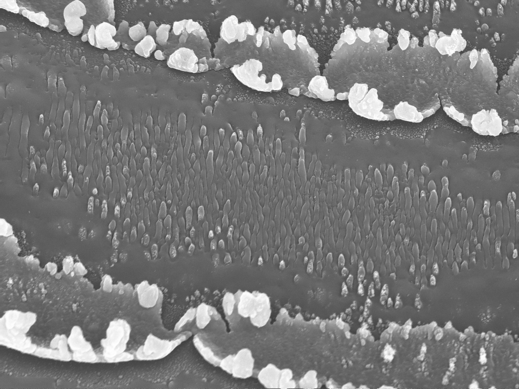 Fig. 10.1 SEM
image at 40° tilt.
Fig. 10.1 SEM
image at 40° tilt. 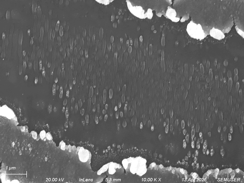 Fig.
10.2 Animation of the tilt
sequence.
Fig.
10.2 Animation of the tilt
sequence. 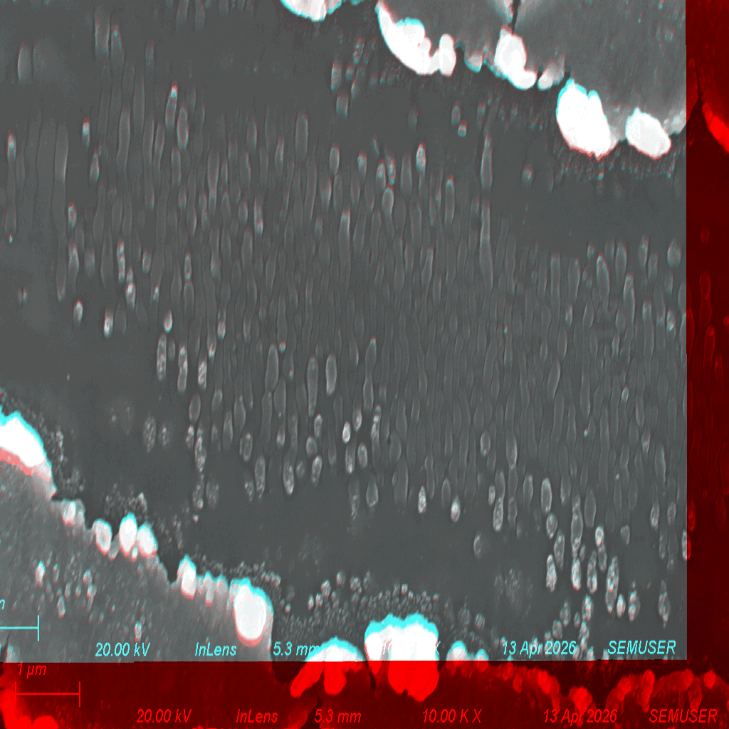 Fig. 10.3 Animated
anaglyphs of the tilt sequence.
Fig. 10.3 Animated
anaglyphs of the tilt sequence. Conclusion
We were succesfully able to generate 1D and 2D periodic structures on both the quartz and glass substrate. Furthermore, imaging the intermediary nano-strucutres formed provided insight into the formation mechanism as expected. However, to further improve on these results, flat top beam should be used instead of a Gaussian to ensure similar structures throughout the beam spot. Furthermore, the fluence used should be more carefully controlled to avoid complete ablation of the substrate.
Acknowledgements
I would like to thank Sean O'Neil and Greg Madejski for the incredible help I recieved throughout the semester. Furthermore, I would also like to thank all the members of the Guo Group, specifically Binod Bhatt for his help with sample preperation.
AI Disclosure
Portions of the HTML and CSS code for this website were generated and/or modified with Google Gemini 3 Flash. The contents of the website, including text and images, are the author's own work.
References
[1] Jihua Zhang, Cong Cong, Chunlei Guo; Single-step maskless nano-lithography on glass by femtosecond laser processing. J. Appl. Phys. 127, 163102 (2020).
[2] Gennady Miloshevsky 2022 Modelling Simul. Mater. Sci. Eng. 30 083001.
[3] S. Nolte, C. Momma, H. Jacobs, A. Tünnermann, B. Chichkov, B. Wellegehausen, and H. Welling, "Ablation of metals by ultrashort laser pulses," J. Opt. Soc. Am. B 14, 2716-2722 (1997).
[4] Anisimov S.I., Kapeliovich B.L., Perelman T.L. Electron emission from metal surfaces exposed to ultrashort laser pulses. J. Exp. Theor. Phys. 1974;39:375–377.
[5] Stuart, B. C., et al. (1995). "Laser-Induced Damage in Dielectrics with Nanosecond to Subpicosecond Pulses." Physical Review Letters 74(12): 2248–2251.