Research Questions
How does EBL exposure dose affect the quality of patterned ring resonators? Is there a specific effect on curved patterns (the ring), small features (like the gap size), and linewidth control (the width of the waveguide)?
A study of how electron beam lithography (EBL) dose influence the fabrication fidelity of simple ring resonator structures, with special attention to gap size and dimensional variation.
Accurate pattern transfer plays a critical role in the fabrication of ring resonator devices, where small dimensional deviations can strongly affect device performance. In electron-beam lithography (EBL), exposure dose and feature spacing both influence linewidth control, gap resolution, and structural integrity. In this work, we use simple ring resonator test structures to evaluate pattern fidelity across different exposure conditions and gap sizes.
How does EBL exposure dose affect the quality of patterned ring resonators? Is there a specific effect on curved patterns (the ring), small features (like the gap size), and linewidth control (the width of the waveguide)?
Simple ring resonators with a single bus with different gaps sizes were patterned across several exposure doses using EBL.
Scanning electron microscope (SEM), atomic force microscope (AFM) , energy-dispersive spectroscopy (EDS), and light microscopy (LM) were used to evaluate the pattern fabrication details. A brief image analysis was performed using ImageJ and statistics were calculated.
The steps followed for this project are summarized as follows,
Ring resonator structures of 20 um diameter, and 1 um waveguide width were designed using AutoCAD. Four different gap sizes were considered: 20 nm, 100 nm, 500 nm, and 1000 nm. A set of four resonator with these gap sizes comprises a single dose.
A silicon chip was prepared with a layer of PMMA. Then, patterns were written using EBL across multiple exposure doses. The software WeCAS was used to generate the dose test using the matrix feature. The dose was varied from 400-2300 uC/cm^2 in steps of 100 uC/cm^2.
Light microscopy was used for coarse inspection. EDS was used to confirm lift-off and search for possible contamination. SEM was used for high-resolution dimensional measurements, and AFM was used to evaluate surface as well as for dimensional measurements.
Gap size, waveguide width, and pattern uniformity, were extracted from images and compared across dose and geometry conditions. This was performed on the SEM images using ImageJ and contrasting with AFM measurements.
The main relevant parameters for this experiment are listed below along with relevant extra information.
| Parameter | Information | Extra notes |
|---|---|---|
| Chip | Silicon chip of 6x6 millimeters | ---- |
| Resist | PMMA | Followed fabrication recipe |
| Ring radius | 10 um | Referred to the outer radius |
| Waveguide width | 1 um | The waveguide refers to both the thickness of the ring and the bus |
| Gap values | 20 nm, 100 nm, 500nm, and 1 um | --- |
| Dose range | 400-2300 uC/cm^2 | The increment was set to 100 uC/cm^2 |
| Deposition | 40 nm of aluminum | Using Culver evaporator |
To be more concise, the design of the ring resonators is included in Figure 2. Where both the drawing in AutoCAD for a single dose, including the four different gap sizes is shown. Also, a screenshot of the WeCas software of the schedule file generated for the dose test is shown depicting all the geometries patterned using the EBL tool.
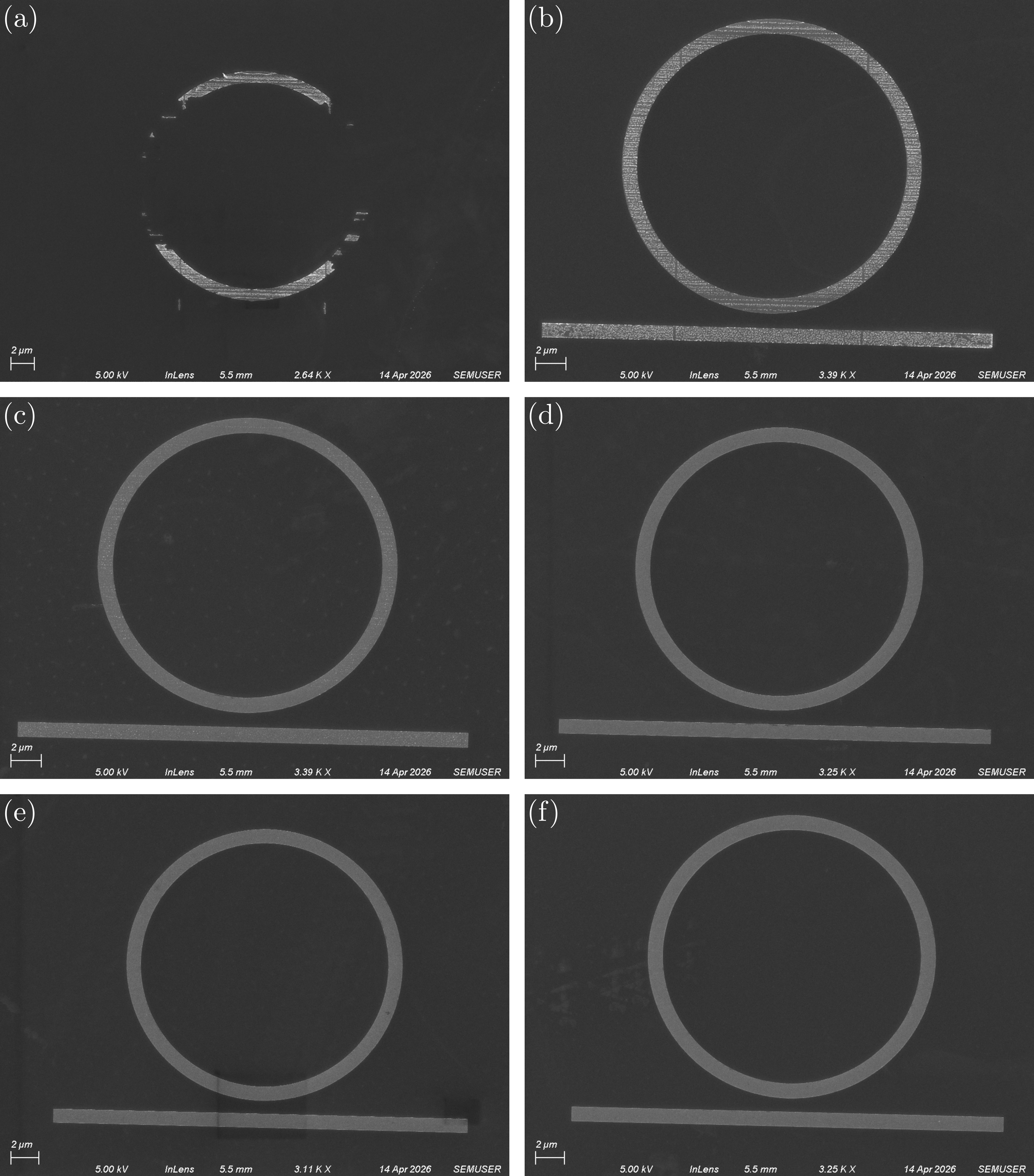
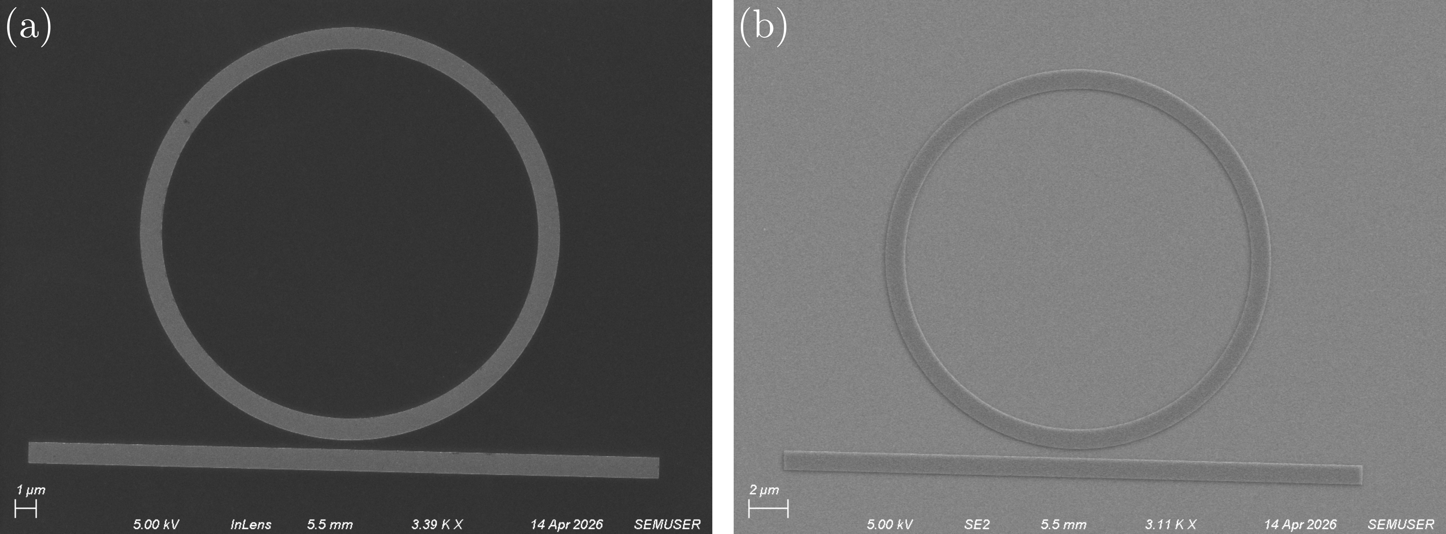
In this section, we report the results obtained from the SEM, AFM, LM, and EDS. After the fabrication, the structures were evaluated using the light microscope, as depicted in Figure 3. One can notice that the lift-off successfully deposited the aluminum into the developed patterns. Although this tool is not enough for studying the integrity of the structures. Figure 2 shows a close-up image of a ring resonator using secondary electrons, more specifically, the Everhart-Thornley detector (SE2) where the ring, bus, and gap are depicted. In the next section we show a full characterization using different tools.
Firstly, energy dispersive spectroscopy provides chemical information of the components in the sample. So it is an useful tool to verify the fabrication process; both the aluminum lift-off and possible presence of contaminants. The results from EDS are contained in the following table:
| Element | Weight % | Atomic % | Error % |
|---|---|---|---|
| C K | 3.96 | 8.7 | 16.49 |
| O K | 1.47 | 2.43 | 14.06 |
| Al K | 1.4 | 1.37 | 16.56 |
| Si K | 93.16 | 87.5 | 6.13 |
We observe the presence of Si and Al as expected from the fabrication, but there are also organic components being detected. This may be due to both PMMA or acetone residues on the chip. Effects from this contaminant will manifest during the SEM imaging. It is also useful to obtain elemental maps for the sample. This is shown in Figure 2(a)-(d) for Al, Si, O, and C, respectively. It it noticeable in both the Al and Si map that the fabrication worked as expected, although residue of Al in the surface is also present. Also, we observe an almost uniform presence of contaminants in all the surface of the chip, again, likely to either dry acetone of residue of the PMMA mask. Figure 2(e) shows the EDS spectrum, and notice that the Al peaks is quite small compared to the contaminants, so we expect to see effects from this in the characterization.
Now, for the SEM characterization we image using secondary electrons, and we have access to both the SE2 detector and the in-lens. Since the in-lens will give an image directly from above the sample without perspective, this is preferred to later extract the dimensions of the structures using ImageJ. In Figure 5. we show the difference in structure integrity across different doses. Notice that for a very low dose we won't be able to expose the PMMA enough, resulting in an incomplete pattern. Notice that a difference of 100 uC/cm^2 is enough to have an actual structure, when comparing Figure 5(a) and Figure 5(b). This tells that the features will be extremely sensitive to the dose. Notice that from 700 uC/cm^2 and above even though we have proper structures, some artifacts are present which can also be seen as roughness of the surface. This reduces drastically from Figure 5(d) to higher doses. Notice as well that there is presence of stains in the substrate, this is likely the acetone or PMMA detected on the EDS results. It is also worth noting that contamination squares can be observed, especially in Figure 5(e) resulting from this contaminants. Other than that across the different doses with structure integrity at this scale is complicated to note any other difference.
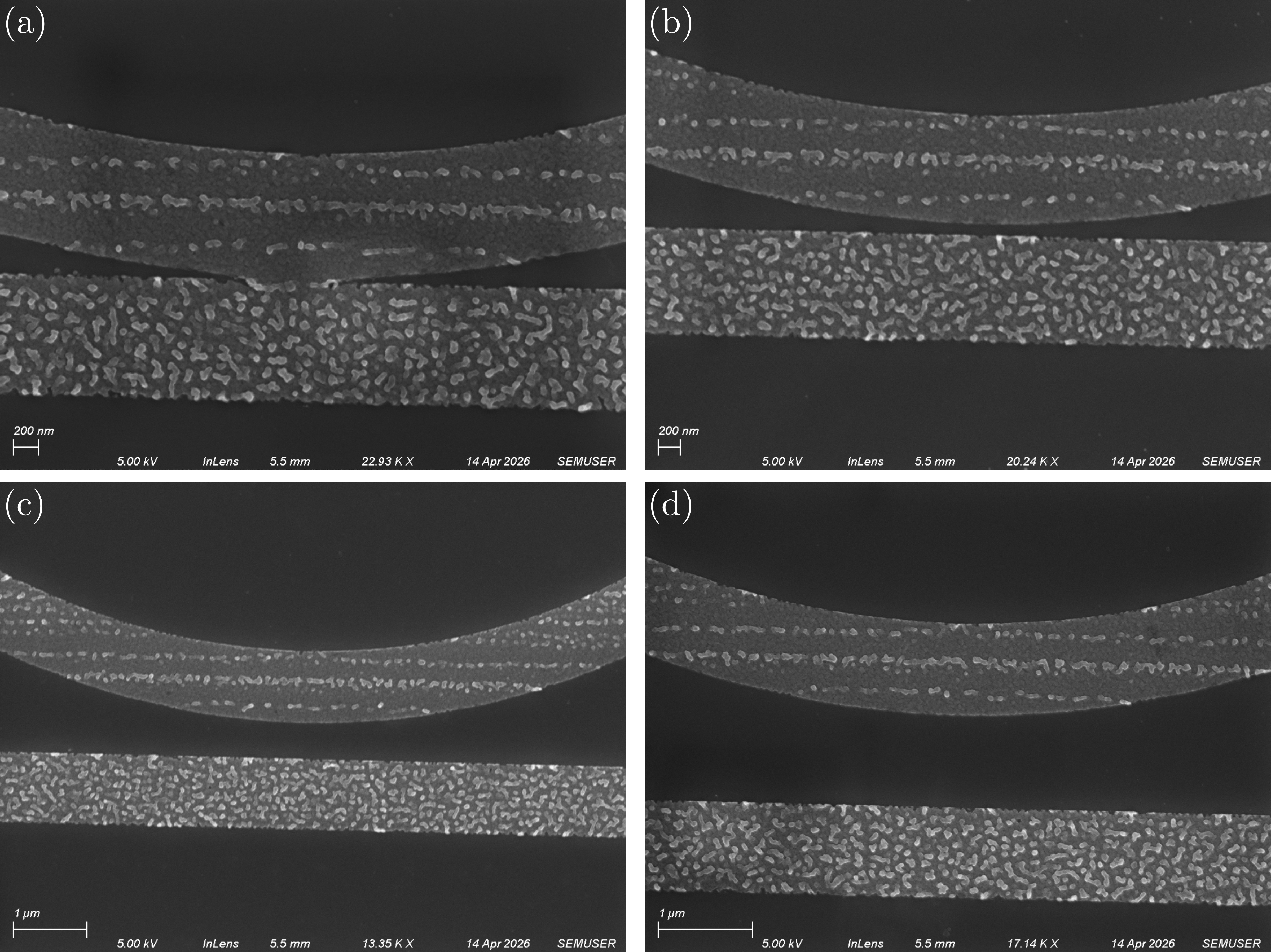
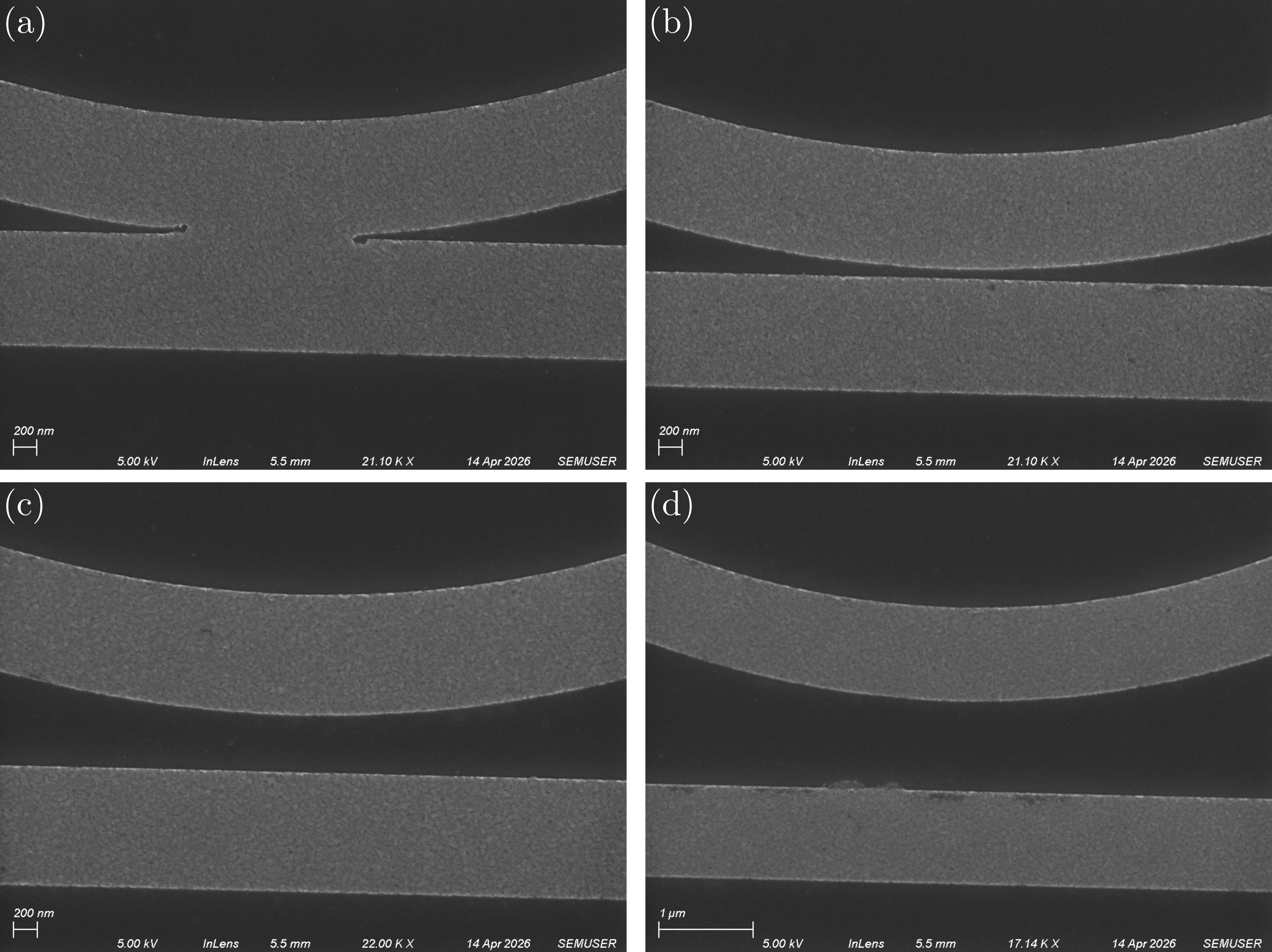
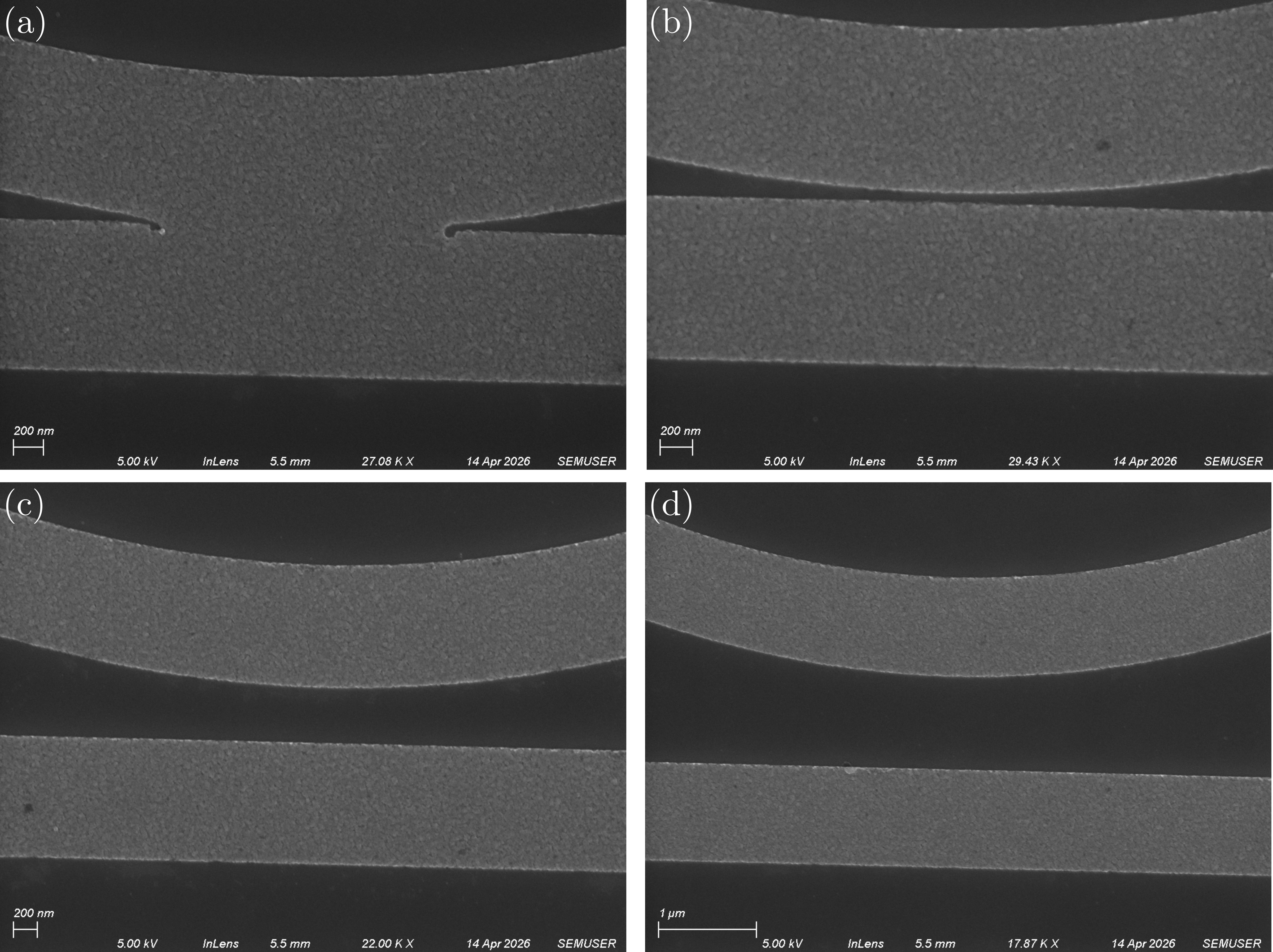
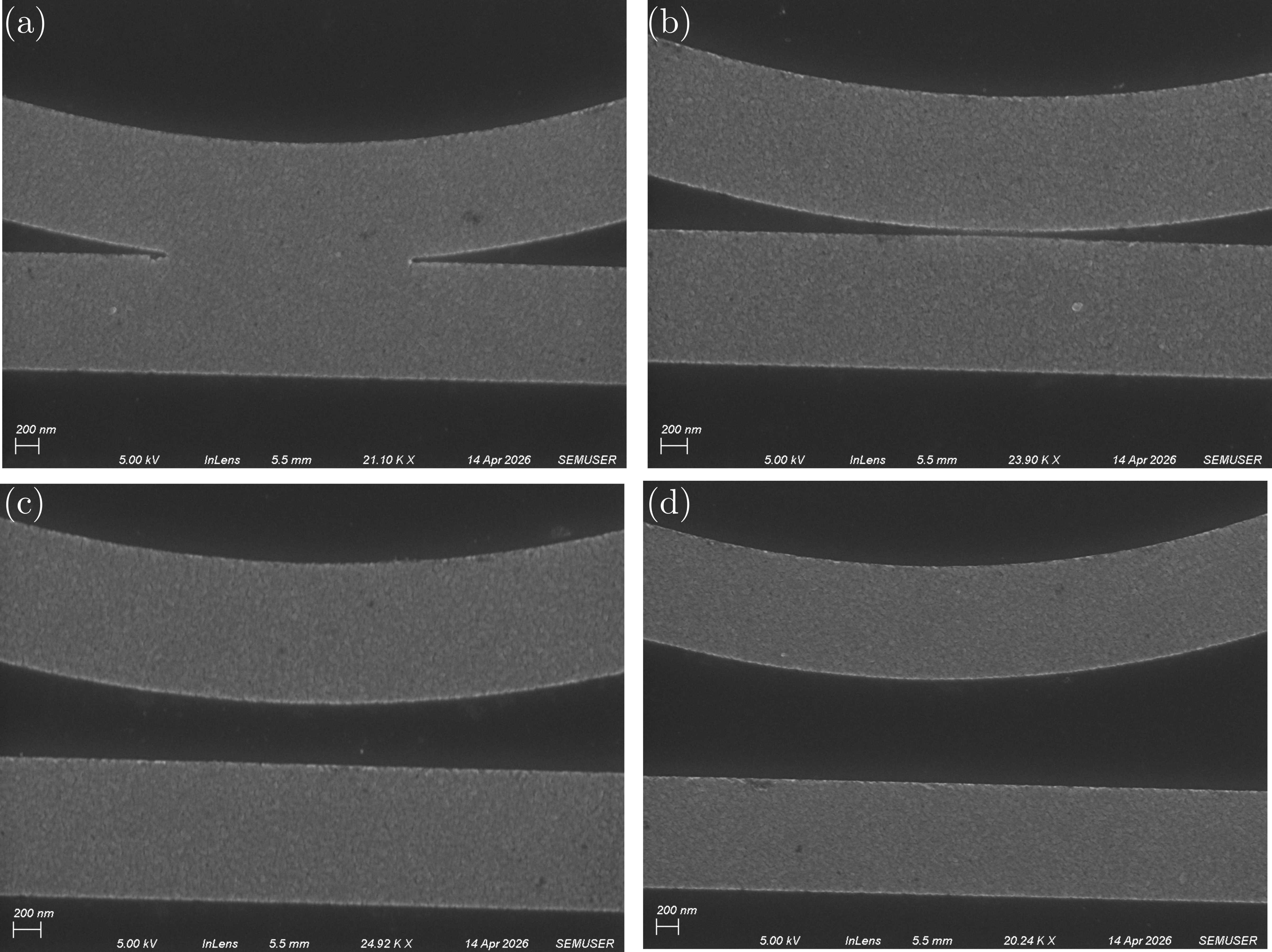
If we now focus on the gap size, which in this design comes to be the smallest feature, we should be able to distinguish the effect from different exposure doses. Below, we show SEM images zooming in into the resonator gaps for the different designed gap sizes for different exposures. The first thing to notice is that none of the exposures were capable of producing a separation between the ring and the bus for the 20 nm gap. This might be due to the current used during the EBL patterning procedure. We then consider the measured gap to be zero for this designed gap size. Next, notice that for a exposure dose of 700 uC/cm^2 shown in Figure 6, the grain size of the aluminum is very noticeable along with defects in the depositions associated to the EBL patterns since these resemble how WeCAS triangulates the design into polygons. When increasing the dose, this grain size decreases but there is presence of some of the grain in the substrate as clearly observed in Figure 7(c), this was expected from the EDS elemental maps results shown above. If we keep increase the exposure dose the surface roughness cannot be evaluated from these images alone and there is no great distinction among the different doses. Also, little can be said about the gap sizes and the waveguide width without further analysis except that for the 2100 uC/cm^2 dose, in Figure 10(b) one can notice that the 100 nm gap looks narrower than for the rest of doses, this will be evaluated carefully in the analysis section.
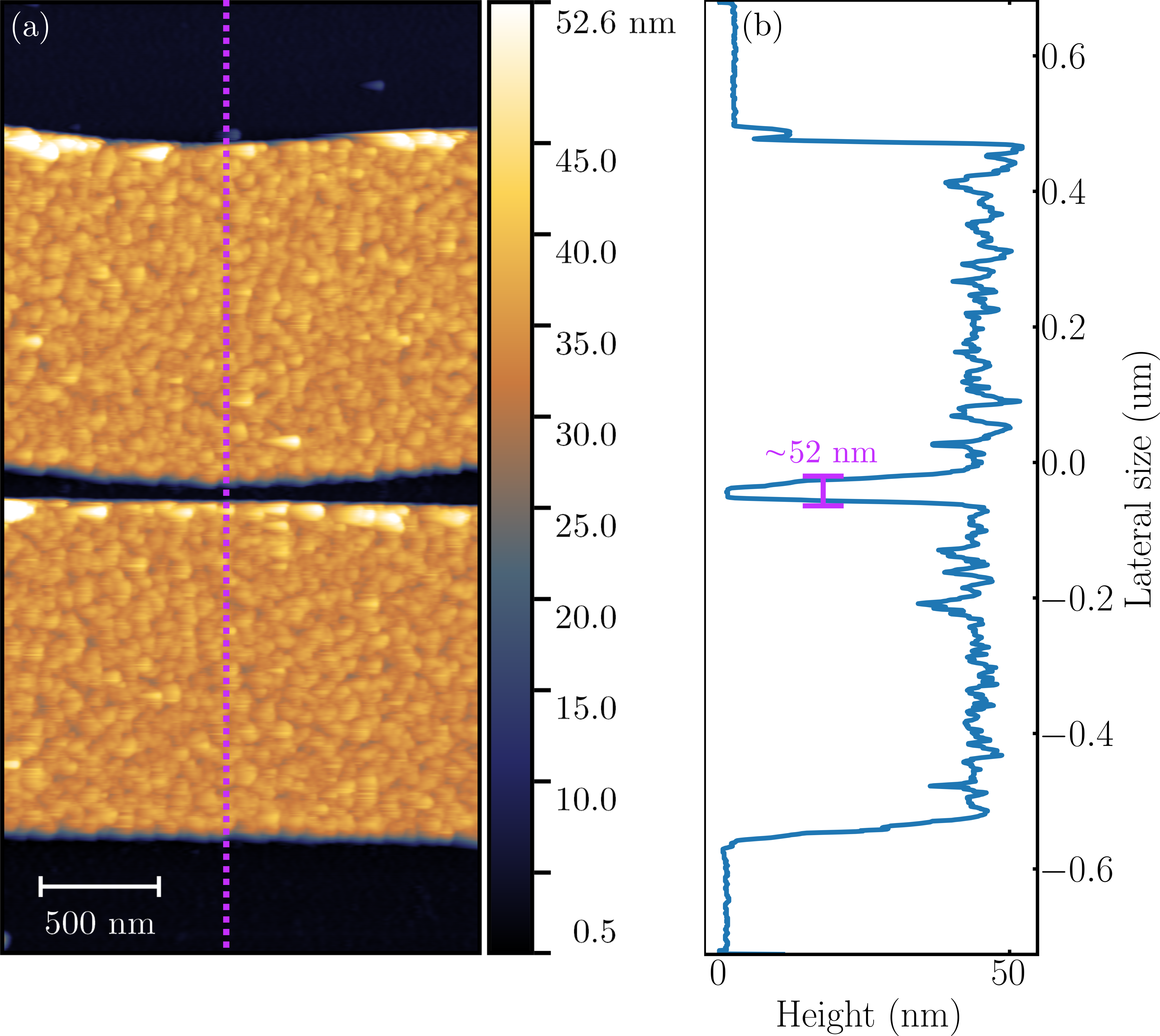
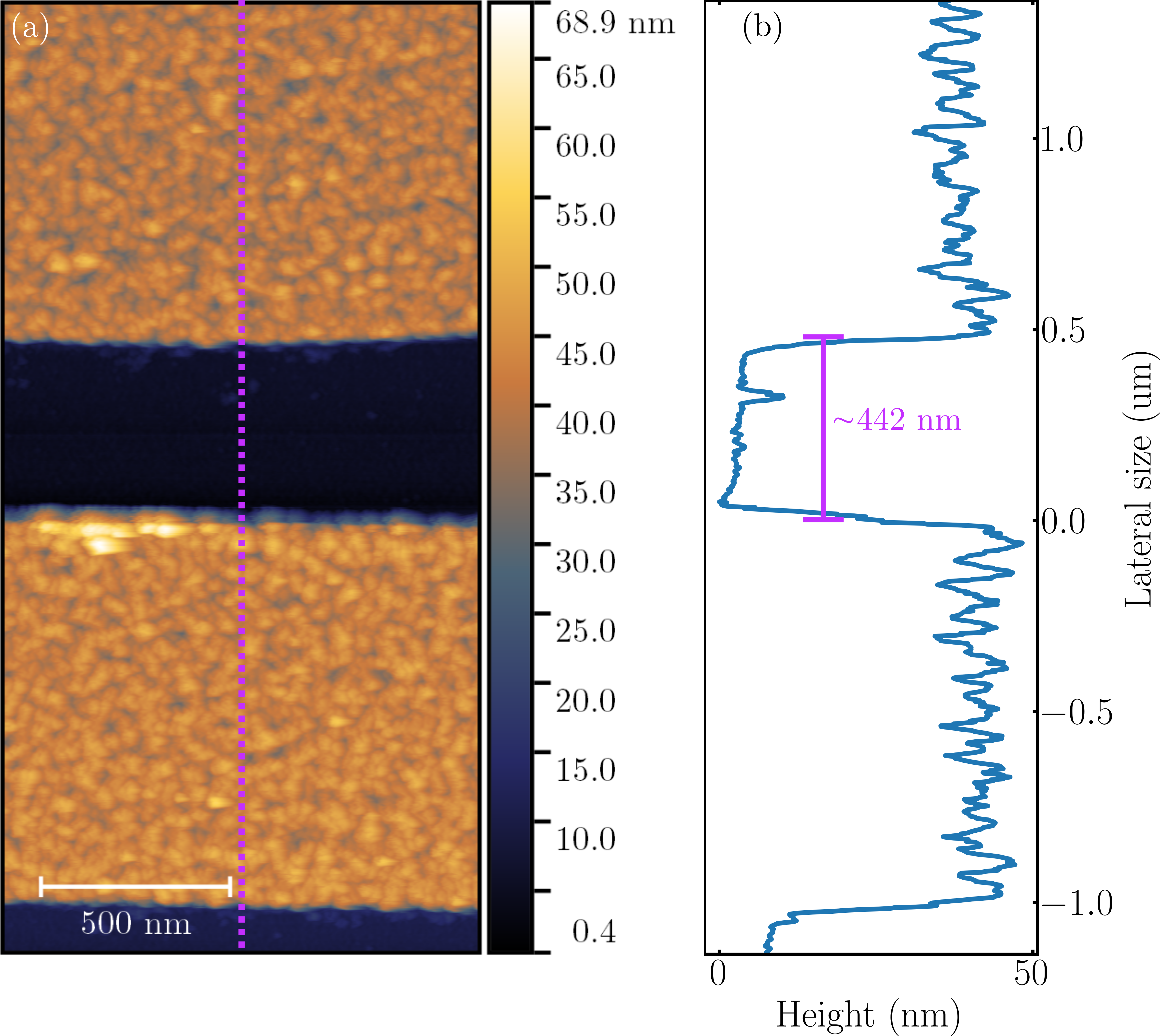
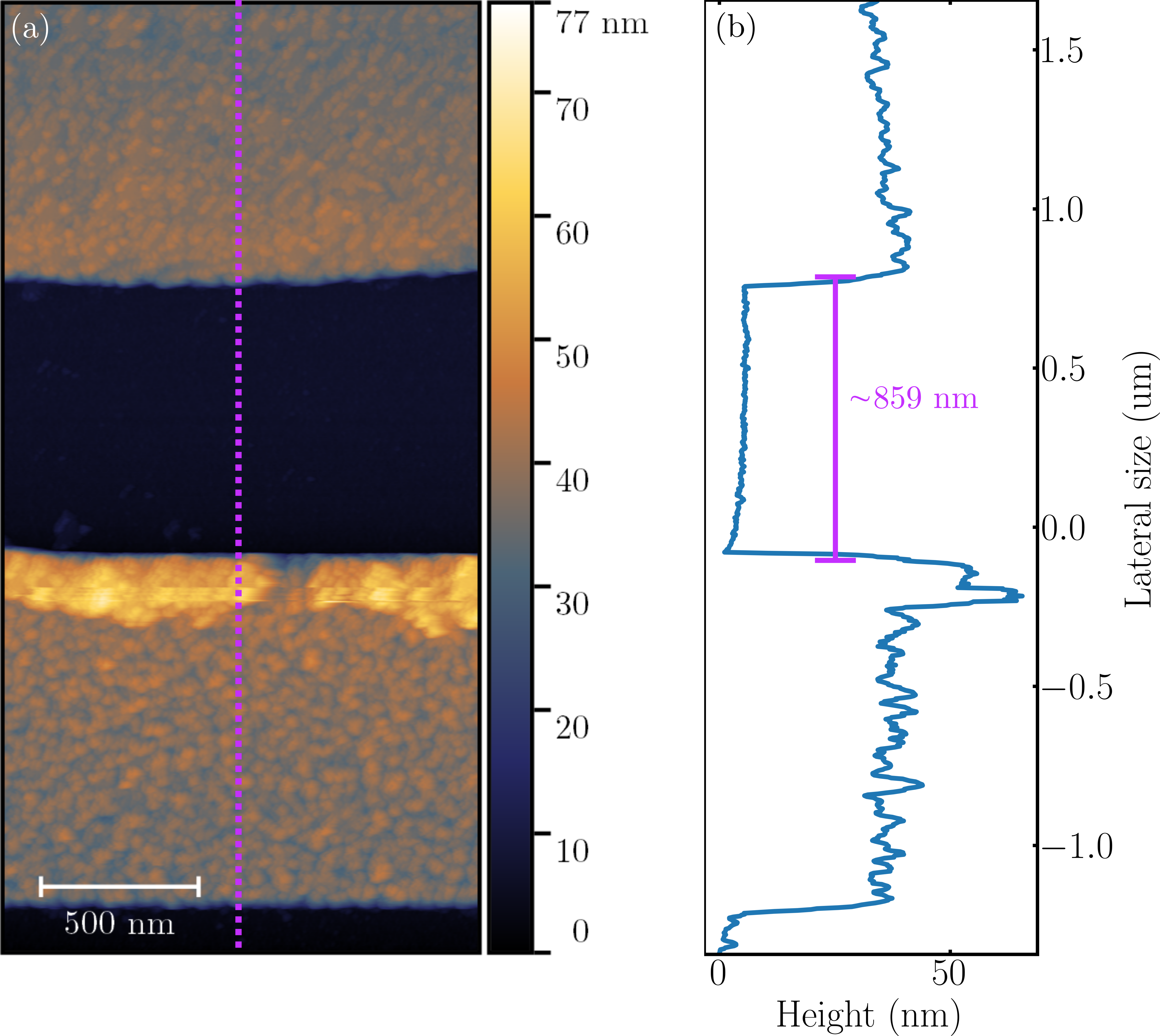
In order to complement the data provided from the SEM that will be analyzed using ImageJ. We use AFM to measure the the gap sizes more accurately. Given to time constraints, only data for the 1200 uC/cm^2 exposure dose could be retrieved. So no other comments about the surface roughness will be given. Also, no data was taken for the 20 nm designed gap size as from the SEM images it can be seen there is no separation between ring and bus. Below, data taken for the rest of gap sizes along with a 1D cut can be observed with estimated measured gap sizes. This was performed using Gwyddion. The main thing to notice is that in all three Figures 11(b), Figure 12(b), and Figure 13(b) the measured gap has a considerable error respect to the designed gap size. In the 2D scan it is also noticeable tha the grain size seem to be homogeneous as seen from the SEM images and notice that the three images have some spikes at the boundaries, specially in Figure 13(a) and Figure 13(b). It possible that this effect is a result of a mix of a bad calibration of gain in the AFM, along with some issues during the fabrication. This needs further study of the rest of the exposure doses to confirm. The data from the gap sizes will be contrasted with the SEM analysis in the next section.
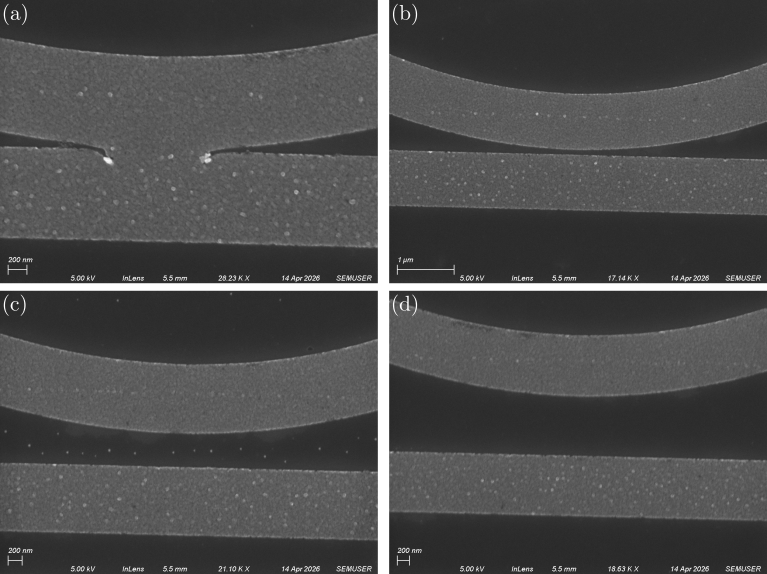
For completeness we show the difference in imaging modes between the SE2 and the in-lens detector for the SEM. The main points observed are the following:
Now, will all the data taken from the SEM images using the in-lens detector, we used the software ImageJ to measure the outer radius, inner radius, waveguide width and gap sizes. A percent error is calculated respect to the designed parameters for each gap size, and for all different exposure doses. Also, these are compared with the AFM results with the only purpose of knowing to which degree are these results reliable.
A summary of the statistical finding is shown in the Table below. Notice that for the designed gap size of 20 nm there was no physical separation, hence the percent error is 100% which is taken into account for the average statistics included in the table below.
| Dose (uC/cm^2) | Outer radius average percent error (%) | Inner radius average percent error (%) | Gap size average percent error (%) | Waveguide width average percent error (%) |
|---|---|---|---|---|
| 700 | 5.399 | 5.405 | 27.920 | 5.347 |
| 900 | 4.992 | 5.030 | 33.545 | 4.646 |
| 1200 | 4.998 | 5.141 | 36.402 | 3.715 |
| 1800 | 5.688 | 5.948 | 41.228 | 3.349 |
| 2100 | 5.247 | 5.626 | 45.905 | 1.837 |
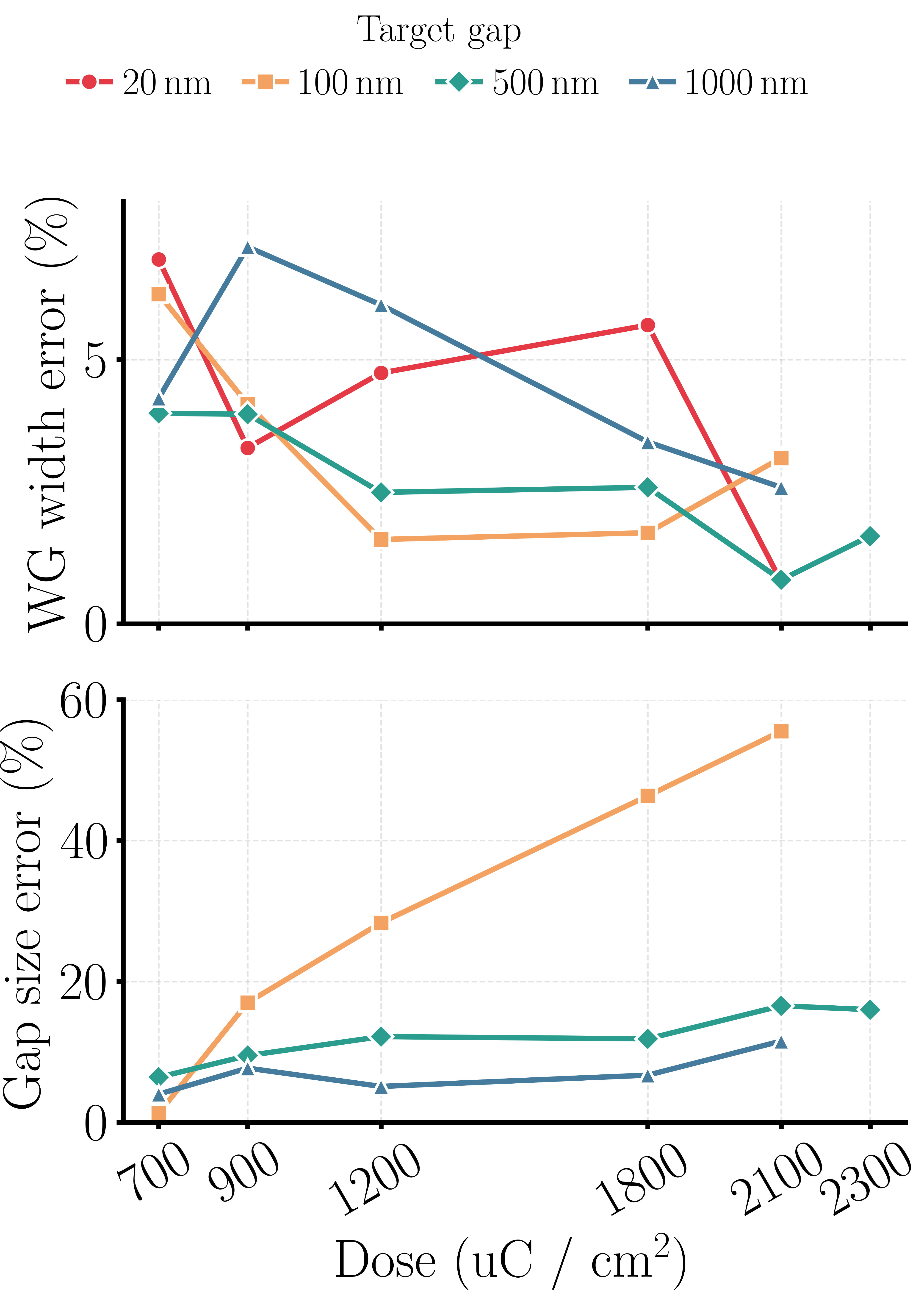
From the table above, two interesting behaviors can be observed, first, among all doses the average percent error for the ring is always around 5%, hence we should only focus in the differences from the waveguide width and gap size. Second, the average gap size has a smaller error for the lower dose, but we now that with such an exposure the surface is rough and presents defects. This is also the dose with higher waveguide width percent error. As we increase the dose the waveguide width error decreases, but the gap size increases. Hence we should look for the dose that minimizes both errors.
In the Figures below, we show the individual behavior of the gap size error and the waveguide width error for the different doses. This is shown in Figure 15. Notice that the overall behavior for the gap size error is to increase with higher dose, and this is more pronounced for the 100 nm designed gap size. This makes sense as it is a smaller dimensions. On the other hand, for the waveguide width error, the tendency as we saw from the average behavior is to decrease with increasing dose. Although the trend is not entirely clear and it might require more statistics.
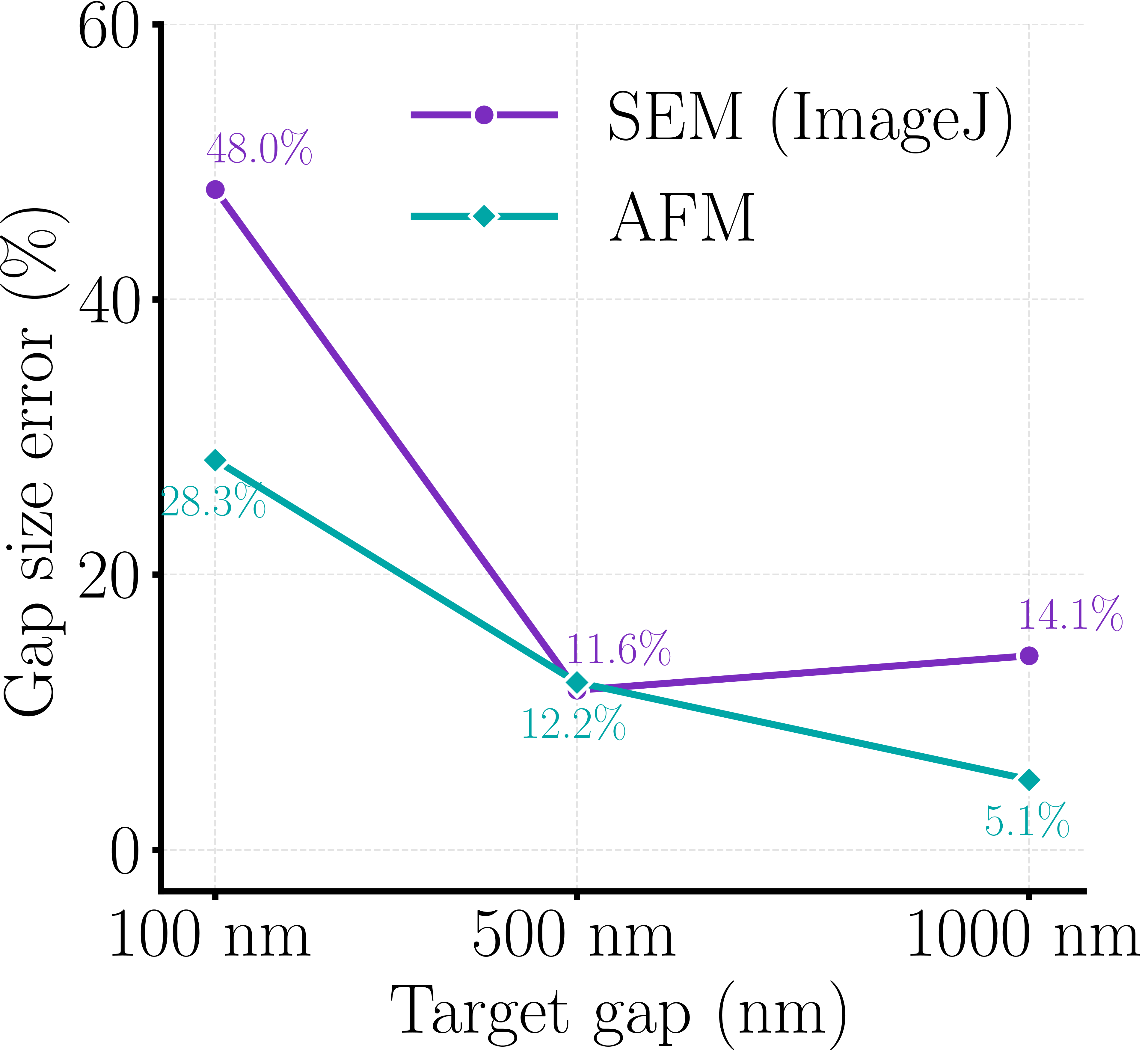
Finally, in Figure 16 a comparison between the AFM and SEM results for the exposure dose of 1200 uC/cm^2 is shown. Here a clear trend is common between both methods, but it is also clear that there is a discrepancy between the error of both methods. There is insufficient data to establish a trend but it is true that the errors are relatively close, so one should be able to trust the analysis from the SEM images.
We evaluated EBL pattern fidelity using simple ring resonator structures with different exposure doses and gap sizes. Both low and high doses affected the final waveguide width and gap dimensions. SEM/ImageJ provided quantitative measurements of lateral features, contrasting the ones obtained using AFM. The differences between both methods show the importance of using complementary characterization techniques. More data is needed to identify definitive trends and to choose the optimal dose for these ring resonator structures. With the current data the gap size error seems to increase with the dose and the waveguide width seems to decrease with increasing dose.
EBL exposure dose has a fundamental effect in the quality of patterns. Both in the accuracy and surface roughness. For these structures gap size error seems to increase with the dose and the waveguide width seems to decrease with increasing dose.
With the current data is not possible to find trends or the optimal dose for the structures. Complimentary AFM and SEM data for more doses is needed.
I acknowledge the Nichol group, especially Suraj Thapa Magar, Jake Markowski, Malick Gaye, Zhengyang Zhang, and Habitamu Walelign for helping me with the fabrication. Also, I thank Sean O’Neill and Greg Madejski for the support and advice for this project as well as the help using the tools.
Portions of the HTML and CSS code for this website were generated and/or modified with ChatGPT 5.4. The contents of the website, including text and images, are the author's own work.