Malick A. Gaye, Nichol Group, Department of Physics & Astronomy, University of Rochester. Spring 2026.
In recent years, quantum technologies have become increasingly promising platforms for both computation and the probing of microscopic physics. In particular, a strong scientific community has emerged behind fabricating and studying silicon-based quantum dot devices. The fabrication of multi-layer quantum dot devices is a very intricate process with many points of potential failure, especially given that these devices require precisely-defined nanoscale features to work. In the final project for the SEM Practicum course, we study how variations in the [e-beam] lithographic patterning ('topic 1') and metal deposition processes ('topic 2') for Au and Al features can impact our device features. We discuss the underlying mechanisms behind these results, and how they could impact quantum dot device functionality and performance. In doing so, we perform imaging of Au alignment marks and small regions of Al device gates using scanning electron microscopy (SEM) for imaging secondary and backscattered electrons, light microscopy, energy-dispersive X-ray spectroscopy (EDS), atomic force microscopy (AFM).
It is common for lithographically patterned quantum dot devices to feature multiple layers of aligned metal gates fabricated on a silicon heterostructure. These gates have features as small as nanometers wide, and as such, are commonly fabricated by using electron beam lithography (EBL) to expose patterns on a photoresist (PMMA) film which, upon developing, give 'wells' in which one can deposit metal, defining the gate features [1].
In EBL exposures, we deliver an electron dose (from the 'primary beam') to points on the photoresist film. Primary electrons undergo elastic and inelastic scattering in the photoresist, which results in a broadened area-of-effect with respect to the primary beam (the 'interaction volume'). This dose induces chain scission in the polymers (assuming positive tone lithography), making it developer-soluble (as opposed to the unexposed regions). Correctly choosing the dose is critical in producing sharp, robust features. In this portion of the project, we consider the impact of under or overexposing the patterns, by varying the electron beam dwell time, which is proportional to the dose. We do this by fabricating four global alignment marks and 18 local alignment marks with linearly increasing doses. We note that the global marks are patterned with a larger beam current and field size with respect to the local marks; however, I will not discuss the exact parameters, as this project is qualitatively-focused. All work for this portion of the project is done on a single chip, and as such, the development, deposition, and liftoff steps of the fabrication are done the exact same way for each pattern.
Our two key lines of questioning are:

When we underexpose our pattern, the electron dose delivered to the PMMA is insufficient in fully inducing chain scission through the volume where we intend to write our pattern. The effect is that substantial regions of the PMMA in the pattern can remain relatively developer-insoluble, meaning that it won't actually wash away during the development step, leaving a thin layer of resist where we intend to deposit our feature. This is called scumming.
As we deposit metal onto scummed regions of the pattern, it doesn't make good (if any) contact with the substrate. Rather, the metal is deposited onto the photoresist film itself. After deposition, when we perform liftoff, this film is washed away in the solvent, taking away the metal's 'foundation' with it. Think of this like gluing two objects together, then dissolving away the glue -- this is going to completely 'unstick' the metal features from the chip, and you'll lose some of your features during liftoff.
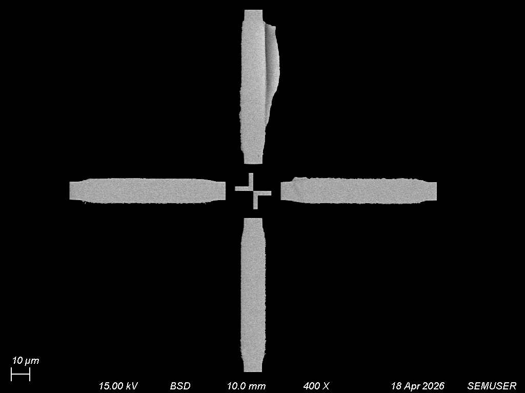
Global mark gA. The center cross is missing and the southern arm is peeling off.
Relevant features:
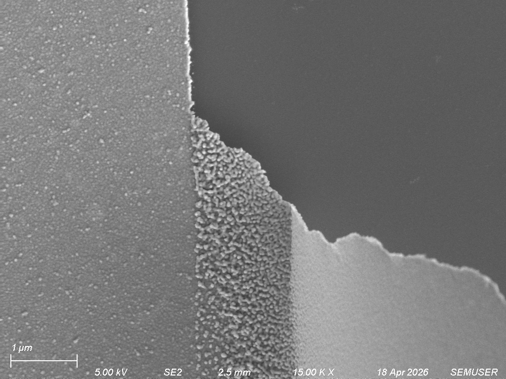
In many of the images for the underexposed features, we see a distinct porous/'bubbly' texture on the metal features; this is most prominent in global alignment mark gA and local alignment marks D13A/B, which received very small electron doses (but enough such that the features didn't immediately wash away). This is explained by the outgassing of the scummed PMMA during deposition. Recall that these features were deposited in the thermal evaporator, in which hot metal gas would make its way up to our chip in a low-pressure chamber and coat its surface. The combination of a low-pressure environment and hot gas heating it up causes the thin residual PMMA layer to start outgassing during the deposition; this means the PMMA is 'bubbling through' the metal as it deposits, creating the structure that we see in the underexposed features. There is likely some contamination involved as well, which could also impact the structural integrity of the feature.
Another qualitative result of underexposures can be seen specifically in the global mark gA: notice the orthogonal 'stripes' on both the top and bottom of the gold arms. These 'stripes' just so happen to be aligned with the chip axes. My hypothesis is that this arises from the electron beam exposing the pattern by exposing at discrete spots ('dots') in a linear grid (a dot matrix). In theory this would result in a spatial periodicity in the dose, which could change the local volatility of the scummed PMMA as well as its developer & acetone solubility. This could mean the gold is being deposited on a 'wavy' (i.e., height-varying) surface after development, and/or that there's periodicity in the amount of PMMA outgassing and thus in the amount of gold 'bubbling'. Either of these cases would result in the axes-aligned 'stripes' that we see on gA. However, the dot spacing for this exposure was 2.5nm, but this is not reflected in the spacing between these stripes. I believe this is due to the large size of the gold grains relative to the 2.5nm interdot spacing, meaning that periodicity in the dose can only be visually seen at scales on the order of the grain size, or larger. Think of the grain size as coinciding with the inverse of the spatial Nyquist frequency (i.e., smaller clumps → higher Nyquist frequency), and by looking at the surface, we're seeing some lowpass-filtered function of the dose.
Hints of 'stripes' on gA could arise from periodicity in the dose.
The results of our 'waxing' experiment reveal that metal features with this morphology are very weak with respect to properly-exposed features. On severely underexposed features such as the local marks D13A and D13B, we see extensive cracking and outright missing chunks of the arms, coinciding with where we did the test searches (i.e., where we ripped off the crosslinked PMMA strips during sonication). As such, these marks are completely unsuitable for use in fabricating a device. One could imagine using underexposed marks for patterning a single gate layer, but since this would introduce crosslinked PMMA strips onto the marks, there's a good chance you'll destroy the mark during liftoff via 'waxing', leaving nothing to align to while patterning the next gate layer.
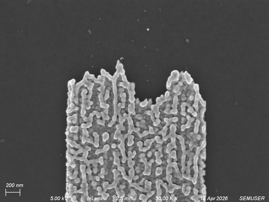
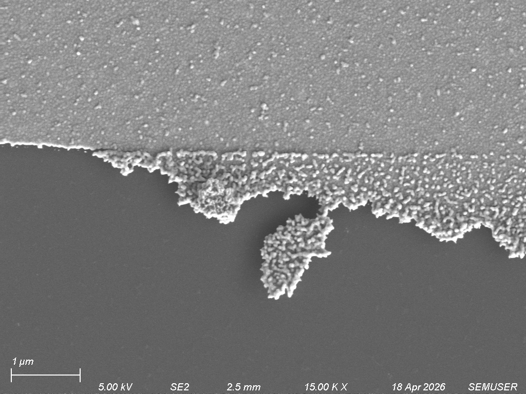
Local mark D13A is abysmally fragile. Both images show that large portions of the arms have torn off during 'waxing' (sonication).
Relevant features:
In ideal doses, our features are characterized by sharp edges, smooth surfaces (i.e., no 'bubbling'), minimal contamination from residual PMMA, and high structural integrity (i.e., minimal 'waxing' damage). This is because of the lack of scummed PMMA where we intend to deposit, giving us smooth, uniform metal with no 'bubbling' artifacts and less PMMA contamination. Well-exposed features are stronger and smoother since we've eliminated the porosity that impacted the underexposed marks -- this means that crosslinked PMMA cannot adequately 'rip' the feature, highlighting its robustness. There is also not nearly as much risk of delamination since the metal directly contacts the substrate.
Well-exposed local mark D32A. Smooth, robust structure with virtually no 'waxing' damage.
Relevant features:
The clearest artifacts associated with overexposures are often related to the 'shapes' of the developed features, and excess metal. In particular, we typically see 'bulging' edges, which arises from what's known as a 'proximity effect'. We also see metal overhangs in some of our images, as well as some evidence of shredding at the edges of our marks. These edges have a similar 'bubbliness' as we saw in our underexposures. We will discuss possible reasons for these effects in the following subsections.
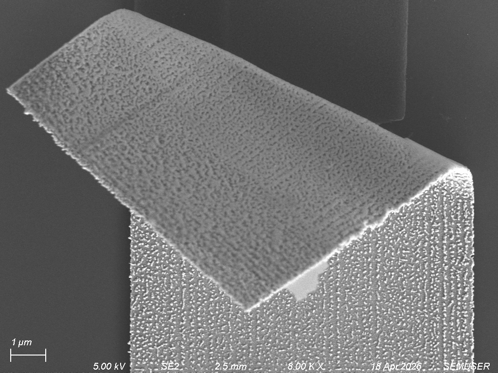
When we expose, we like to think of the beam as exposing at arbitrarily small 'points', but in reality this is not happening. Although the beam spot size is quite small (on the order of nanometers), when the primary beam is shot at the photoresist film, the interaction volume broadens due to forward and backward scattering of the electrons, and secondary interactions that are induced. For example, atoms in the photoresist will 'deflect' electrons, which 'widens' the interaction volume. This widened interaction volume 'reaches' into neighboring regions of the photoresist, meaning it gets a dose where we otherwise did not intend to. The larger the dose, the more 'unintentional' dose neighboring regions get, meaning our patterns get blurry/warped; we lose resolution because we lose the ability to dose precisely at one point, and our patterns start to look like a convolution of the intended pattern with a shape that has a size on the order of the interaction volume. When we deposit here, we'll be left with tons of excess metal, and bulging features.
Think of overexposing like cooking a steak with a flamethrower -- sure the steak will be cooked, but everything else in your kitchen will also be cooked.
Global mark gD is severely over-exposed. We see extreme warping of the edges and tons of excess metal.
Relevant features:

A sketch of what could contribute to the metal overhangs.
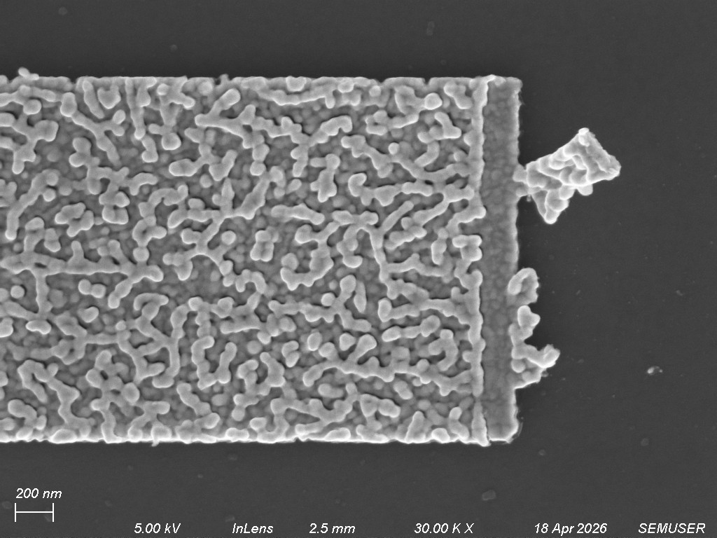
In images such as the one below, we see that the edges of the mark show evidence of violent tearing, leaving some of the metal only tentatively attached to the mark. Also, notice that we can see 'shadows' below these edges -- this means these edges aren't extending down to the substrate, but rather 'overhanging'. This is because unintended regions of the PMMA near the top of the intended features had received a non-negligible dose due to overexposure, meaning that it became developer-soluble and washed away during the development step. This means that we have a depth gradient at the top of the developed film. The deposited metal inherits this gradient, making it more difficult for the unintended metal to break away during liftoff, meaning we're left with metal overhangs.
Now that we understand this, we can infer that the shredding effect is from liftoff itself. Where this occurs is where the metal is thin enough to actually tear apart from the overhang. As we see, it's still too thick for it to occur 'cleanly', and so we get some noticeable damage at the edges. This shredding is also somewhat related to the texture, which we discuss in the next subsection.
On gD, there is clear evidence of shredding at the edges. These edges also have little depth.
Relevant features:
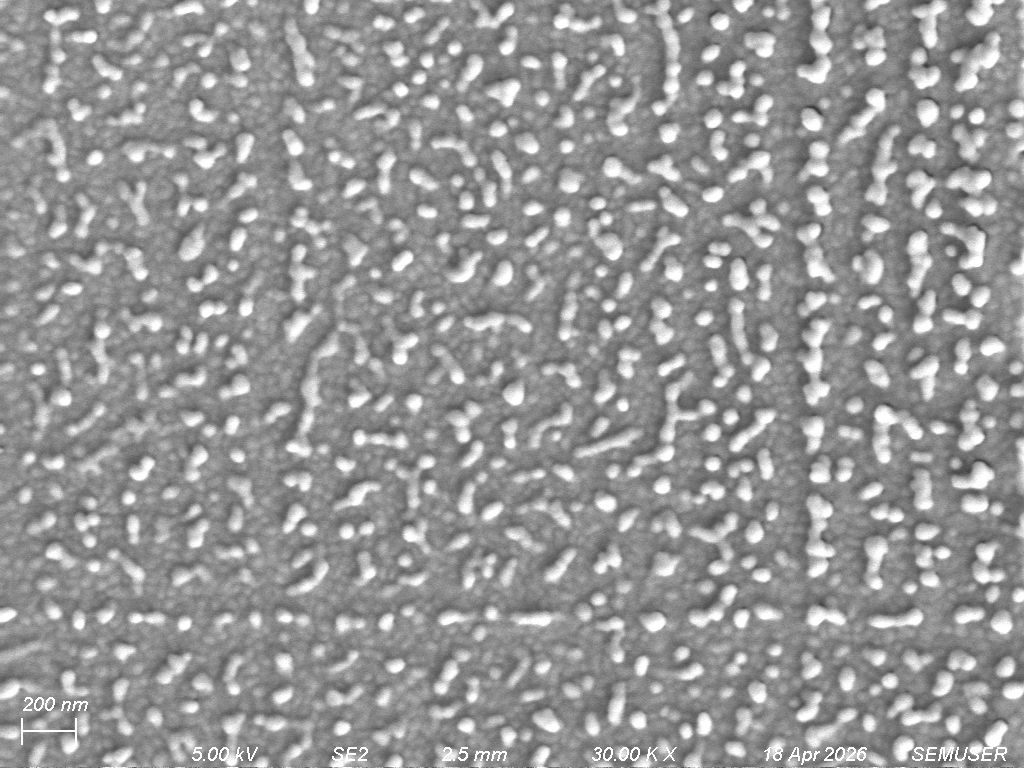
The last major effect of overexposures that we point out is the notable variation in the feature morphology as we near its edges. This can be explained by a couple different things. First, remember that we have thin metal overhangs deposited on slightly-exposed PMMA. This PMMA was not meant to be exposed, but due to overexposing at some neighboring areas, we get an underexposure (with respect to the target dose) at the bulges. As such, we understand this 'bubbly' texture at the bulges to have a similar origin as what we saw in the underexposures: underlying PMMA outgassing and disrupting the metal. As we saw in the underexposure section, when we see this texture, we should expect our metal to be weak, which is consistent with the metal tearing off during liftoff here.
In particular, notice that some of the changes in the texture can be quite abrupt. We could attribute this to variations in the thickness of the metal and/or the amount of PMMA outgassing (e.g., due to being near the pattern edge), which would directly factor into the surface texture. These apparent 'boundaries' could also coincide with mismatches in the mechanical stress, which could explain their sharpness. We leave these ideas to be explored further in the future.

Notable texture variation along gD. Although the edge in the left image appears to be 'folding', note that this is not the case.
Relevant features:
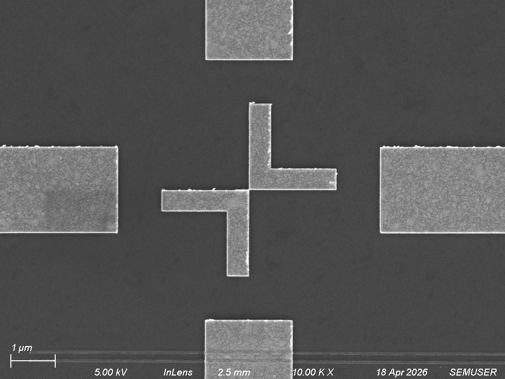
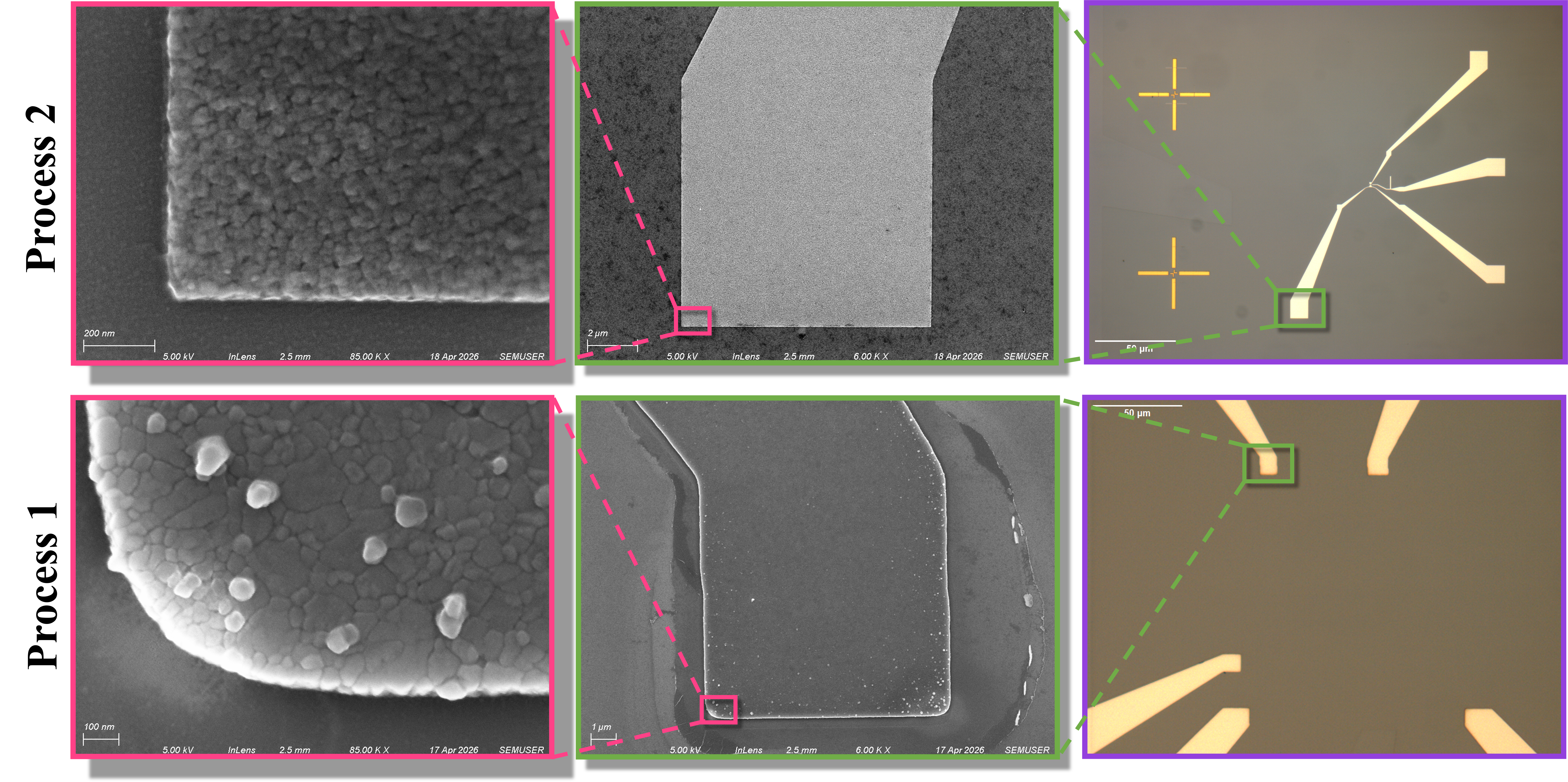
Select a feature on the grid above to reveal descriptions & images. Click directly on the text itself for the feature of interest. Features are lexicographically ordered according to electron dose, with gA and D11A having the smallest global & local mark doses respectively. Note that marks on D11 and D12 are missing due to severe underexposure.
List of clickable features:
In the previous topic, we have found that the dose used in our lithography step can significantly impact the structure, robustness, and fine definition of our metal features. Assuming that we can achieve the ideal dose, we're not completely out of the woods; we still have to perform our metal deposition, and the process we use can concretely impact various material properties of our features. It has been shown that these properties, such as grain size and oxidation profile, can measurably impact quantum device performance [2]. As we will come to see in this portion of the project, our choice of metal deposition empirically changes these material properties (as is theoretically studied in [3]), and so this could mean getting a better or worse-performing quantum dot device with a given process.
Our guiding questions for this section are:
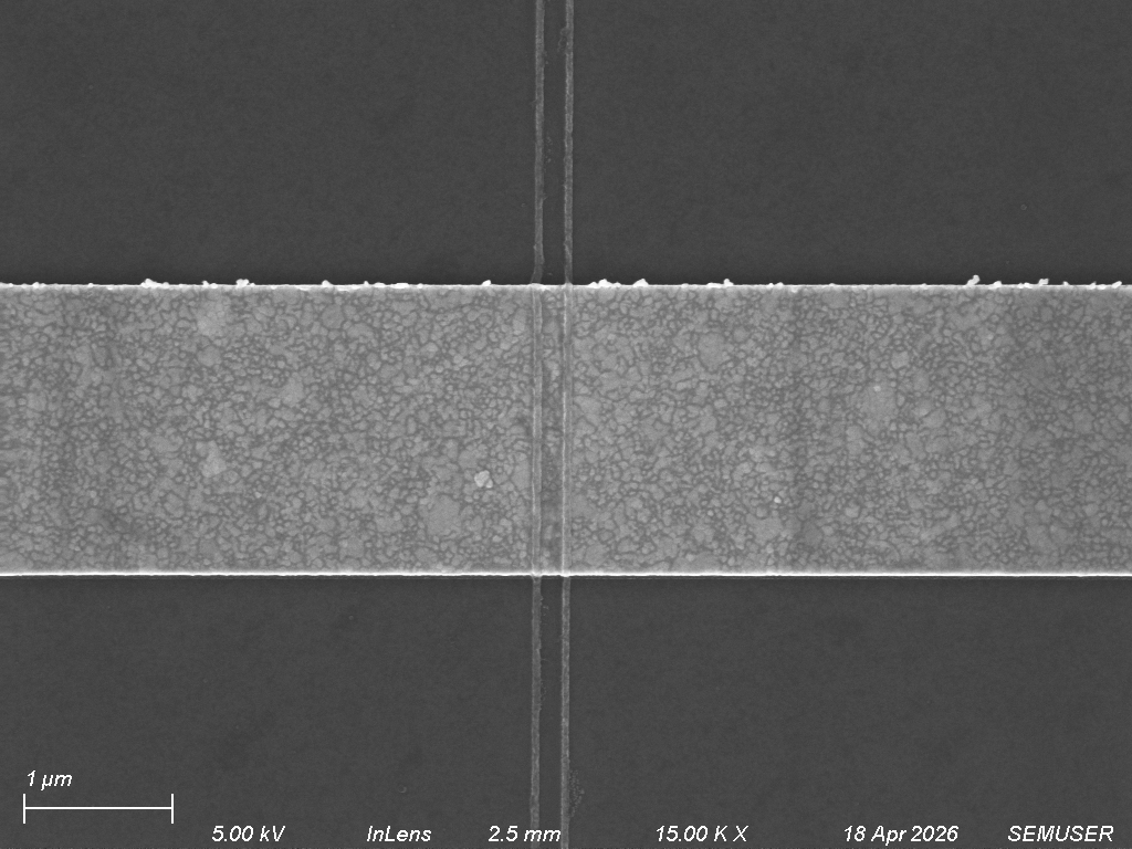
SEM (first two columns) and light microscope (last column) images of the features deposited with process 1 (bottom) and process 2 (top).
We must be careful with our weighting of SEM images in discussing surface roughnesses in particular, as the nonnegligible size of the interaction volume means that signal from below the surface can show up in our images. So, in order to confirm that process 1 results in truly a smoother surface than process 2, we turn towards AFM imaging. AFM in semi-contact mode involves the use of a PID loop to fix the damped deflection of a small tip by vertically moving a sample stage, which helps us reconstruct a height map of the sample (which are the chips in this case). The AFM has a resolution on the order of nanometers, which makes it especially useful for extracting fine surface texture information. We set up a detailed scan with xy-resolution close to the Nyquist limit (about 5nm), and perform the same AFM scan on the features on both chips above.
Critically, we note that AFM data must be processed, as it will have artifacts such as global tilts that prevent us from doing a useful surface roughness analysis. The processing was done in the software Gwyddion; I outline the steps below:
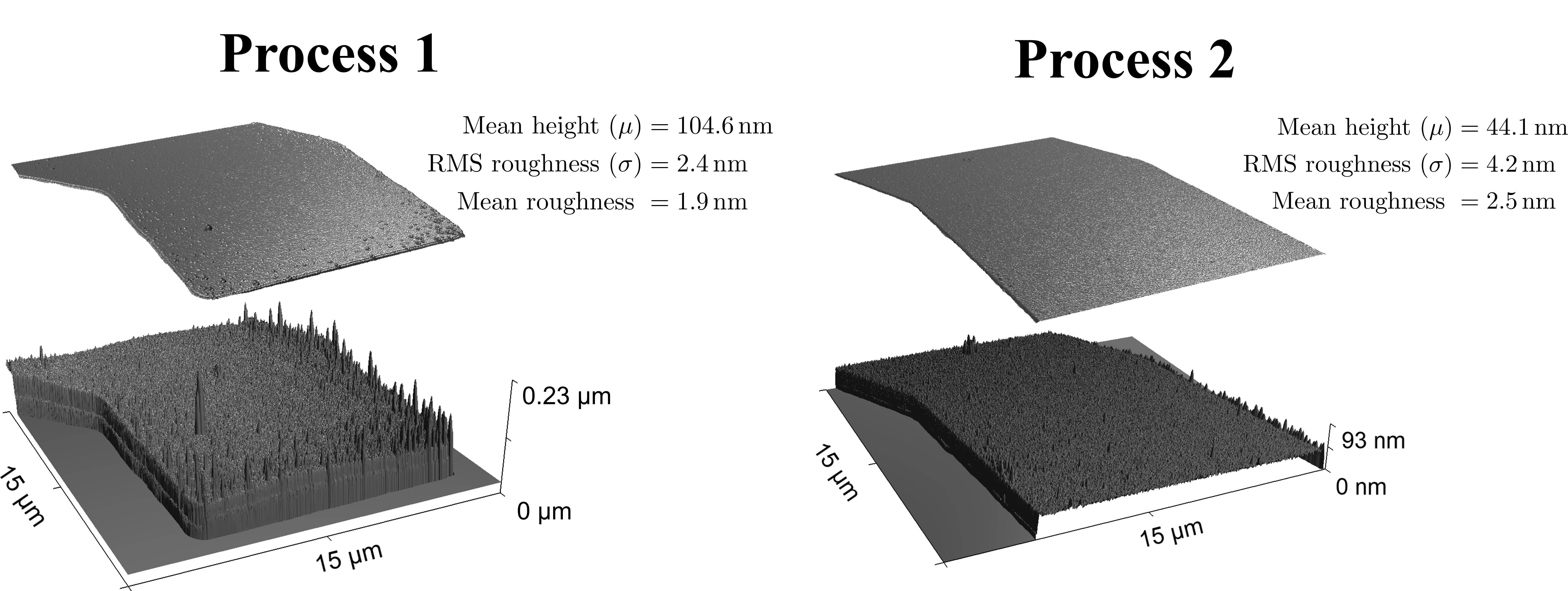
AFM results for both processes. The top views have x:y:z scales of 1:1:1, and the bottom views are exaggerated (1:1:20).
At its core, the fundamental goal of processes 1 and 2 are the same: get Al onto the chip where we've patterned. However, we see that these processes result in clearly different metal film profiles. We find that this is primarily due to the difference in pressure between both evaporators and the means by which the metal is being evaporated. We will discuss these causes in the following subsections.
The reason why thermal and e-beam evaporators are held under vacuum is partially to increase the mean free path of the metal. Metal atoms are liberated from the source at some high energy, making them hot, and they lose this energy to any gas particles that they collide with on the way to the chip. At high pressure, there is a lot of gas, and metal atoms which make it to the chip have lost a lot of their energy to these gas particles. This means these atoms quickly 'freeze' near where they've arrived at the chip, forming small clumps (that we call 'grains'). Conversely, at low pressures, metal atoms can retain much of their energy upon reaching the chip rather than losing it to the gas, which aids in their diffusion across the chip's surface. The result of this is a larger grain size.
As was implied earlier, variance in the grain size has been shown to play into the performance of quantum technologies [2] (this work in particular shows qubits having a shorter relaxation time with smaller grains), and the electrical properties of the feature [4] (in particular, a smaller grain size generally coincides with higher resistance, due to grain boundaries scattering electrons). As such, the grain size can have a non-negligible impact on whether one can successfully fabricate a quantum dot device.
We also note that there are differences in the metal features in the level of contamination. Going back to the notion of chamber pressure, there are more natural contaminants, such as oxygen, as the pressure increases. This means that aluminum oxide can naturally form quicker at a higher pressure as the metal is being deposited. As such, we might expect that process 2 has more aluminum oxide growth per unit time as the metal deposits. Aluminum oxide is an insulator, and thus its presence coincides with decreased bulk conductivity with respect to pure aluminum [4]. Additionally, an increasing amount of aluminum oxide has been shown to correlate with charge noise in Si/SiGe quantum dot devices [5], although the underlying mechanism behind this is not well understood.
Another reason why one process can be 'dirtier' than the other is because of the way in which we evaporate the metal. In a thermal evaporator, we run a very high current across the metal, which heats up the entire source (and neighboring objects, including the boat where it sits). Neighboring contaminants could thus be vaporized and deposited onto the chip, just like the metal source. In the e-beam evaporator, we direct an electron beam at a very specific point on the metal source, causing heating to be fairly localized, and theoretically resulting in less contamination from neighboring 'stuff'. This means that process 1 should also be 'cleaner' than process 2, not only just in the formation of oxides due to the decreased presence of atmospheric gases, but also due to less heating of unintended materials.
Now that we have finished discussion of the two main topics as is within scope for this project, we reiterate our guiding questions and summaries of our findings.
I'd like to give thanks to Sean O'Neill and Greg Madejski for their instruction in the Spring 2026 SEM Practicum course and in providing assistance with imaging for the project. I would also like to thank various members of the Nichol Group for their willingness in discussing device fabrication and the physics of some of these results. In particular I'd like to shout out Jake for training on microlithography and the thermal evaporators, and Suraj for training on the e-beam evaporator and liftoff. I'd also like to thank Dr. Nichol for inspiration of the overall project.
Disclaimer: portions of the code for this website were generated using the Sonnet 4.6 model of the Claude LLM (specifically, for the 'alignment mark viewer'). The contents of the website, including text and images, are the author's own work.
[1] Connors, Elliot. Advancement of Silicon-Based Spin Qubits: Fast Readout, Noise Spectroscopy, and Coherent Control in Si/SiGe Quantum Dots. 2022. University of Rochester. urresearch.rochester.edu, http://hdl.handle.net/1802/37102.
[2] Premkumar, Anjali, et al. "Microscopic Relaxation Channels in Materials for Superconducting Qubits." arXiv, 2020. DOI.org (Datacite), https://doi.org/10.48550/ARXIV.2004.02908.
[3] Qiu, Hong, et al. "Effect of Deposition Rate on Structural and Electrical Properties of Al Films Deposited on Glass by Electron Beam Evaporation." Thin Solid Films, vol. 414, no. 1, July 2002, pp. 150-53. DOI.org (Crossref), https://doi.org/10.1016/S0040-6090(02)00454-6.
[4] Czerwinski, Frank. “Aluminum Alloys for Electrical Engineering: A Review.” Journal of Materials Science, vol. 59, no. 32, Aug. 2024, pp. 14847–92. DOI.org (Crossref), https://doi.org/10.1007/s10853-024-09890-0.
[5] Connors, Elliot J., et al. “Low-Frequency Charge Noise in Si/SiGe Quantum Dots.” Physical Review B, vol. 100, no. 16, Oct. 2019, p. 165305. DOI.org (Crossref), https://doi.org/10.1103/PhysRevB.100.165305.