University of Rochester, Department of Optics
1. Introduction
Quantum computing is becoming one of the most prominent candidates for the next advance in human computational power. As the development of quantum computers advances, the need to store and transmit qubits across long distances becomes an important problem. As many qubit designs only allow interaction between two adjacent qubits, and many algorithms require interaction between distant qubits, the current approach uses SWAP gates to bring two qubits together, which is very expensive. Sending the qubit state into another system that can store and transmit the state becomes a solution to address such problems. By coupling a qubit to a longer-lived system, the quantum state can be stored, transferred across distance, and combined with additional error-correction schemes. Thanks to their piezoelectric coupling, Surface Acoustic Wave (SAW) devices are a very promising platform for this purpose. This project explores the fabrication process and results of SAW resonators on a highly piezoelectric material LiNbO3.
2. Device Fabrication
To effectively couple to spin qubits, the designed SAW resonator needs to resonate at GHz frequencies. This makes the designed resonator have the smallest feature size of ~100 nm spacing. Thus, to successfully fabricate such a device, electron beam lithography needs to be used. In this section, the device design, fabrication process, and final fabricated result will be presented.
I. Device Design
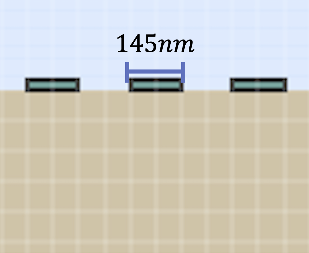
The design principle of the device is straightforward. The target design frequency is 6 GHz, and the acoustic wave speed on LiNbO3 is 3400 m/s. Using these two parameters, we can find that the wavelength of the acoustic wave is 567 nm. The IDT period needs to be half the wavelength to achieve constructive interference. With a 0.5 metallic ratio, the width of the metal strip is 145 nm.
II. Fabrication process
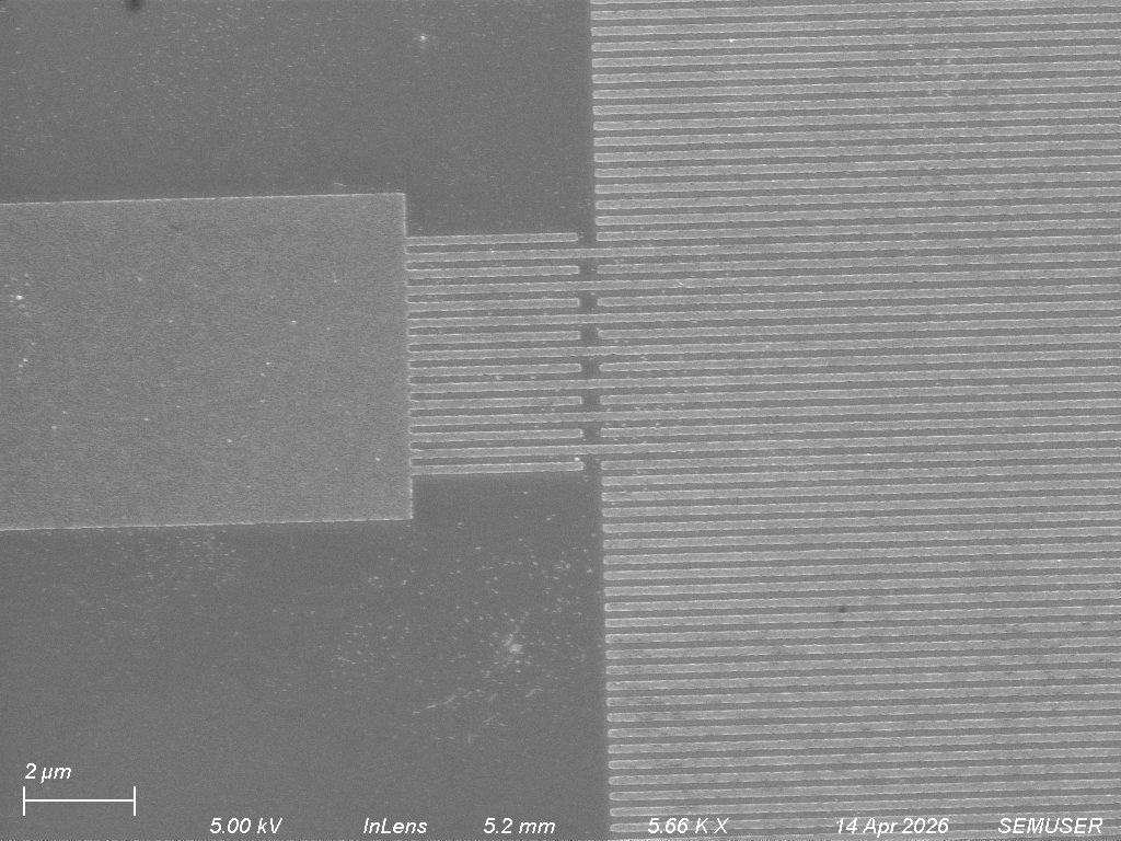
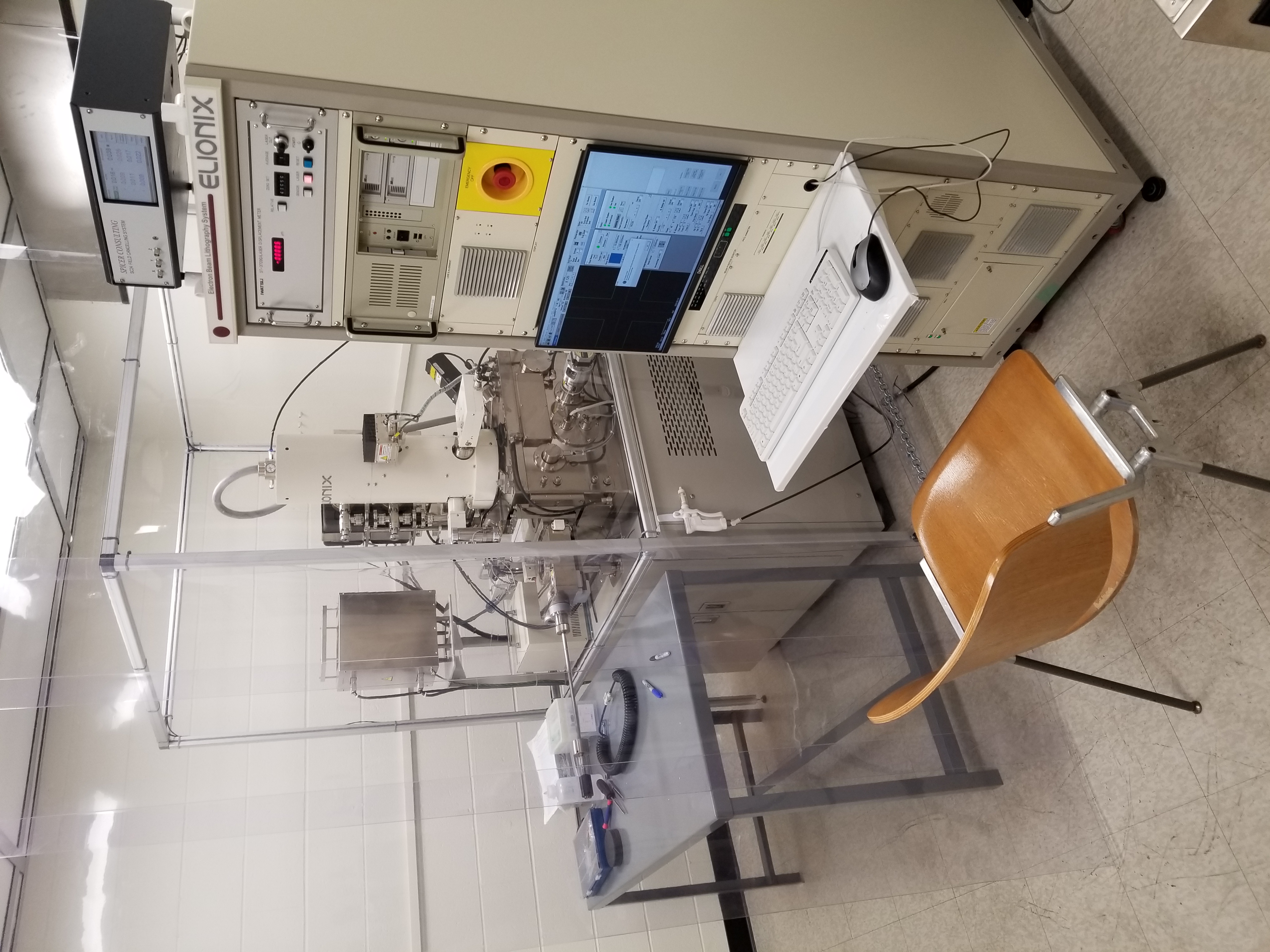
The devices were fabricated through the following process: 1. Substrate preparation — the LiNbO3 chip was descummed, sonicated, and coated with PMMA resist, followed by a discharge-water layer to suppress charge build-up on the LiNbO3 surface. 2. Pattern writing — the design was written on the chip with an Elionix EBL system. The patterned chip was then developed in MIBK/IPA to remove the exposed regions and reveal the pattern. 3. Evaporation & lift-off — the developed chip was loaded into an evaporator to deposit aluminum, then soaked and sonicated in acetone to lift off the resist (and the metal above it), leaving the patterned metal on the substrate.
3. Overdose & Underdose
To properly fabricate the devices, the electron beam dose needs to be carefully adjusted. The devices were fabricated under different doses, and the effects of overdose and underdose were investigated using AFM, SEM, and EDS.
I. Underdose
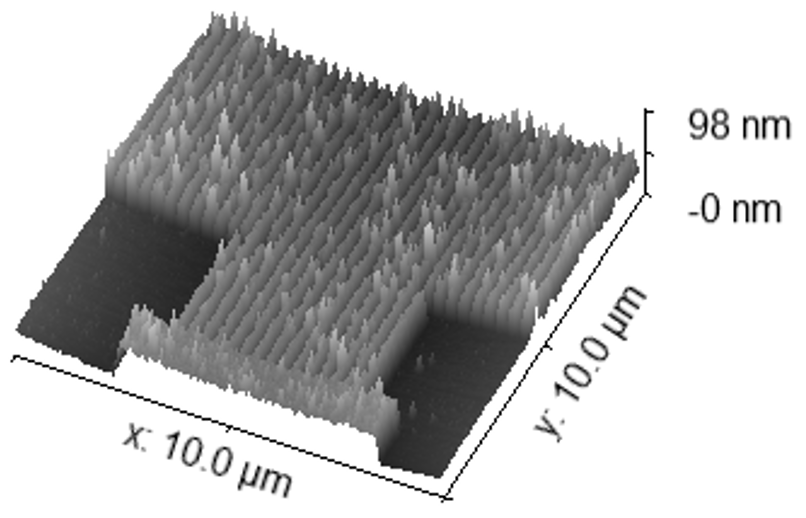
When the fabricated devices were underdosed, the dose incident on the resist was not strong enough to fully expose the pattern. Thus, there was undeveloped resist in the metal-mirror region. This residual resist was covered by the evaporated metal, producing undesired thickness variation. In the AFM image, this appears as small peaks on the underdosed device, and in SEM images they present as small bright dots.
II. Overdose
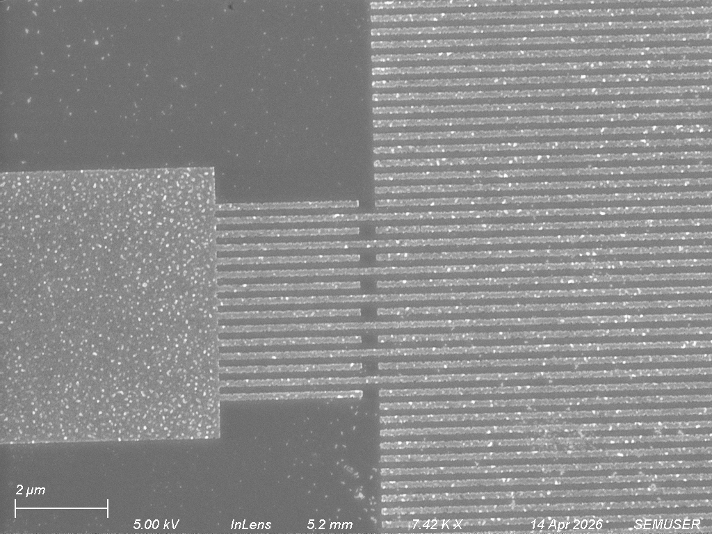
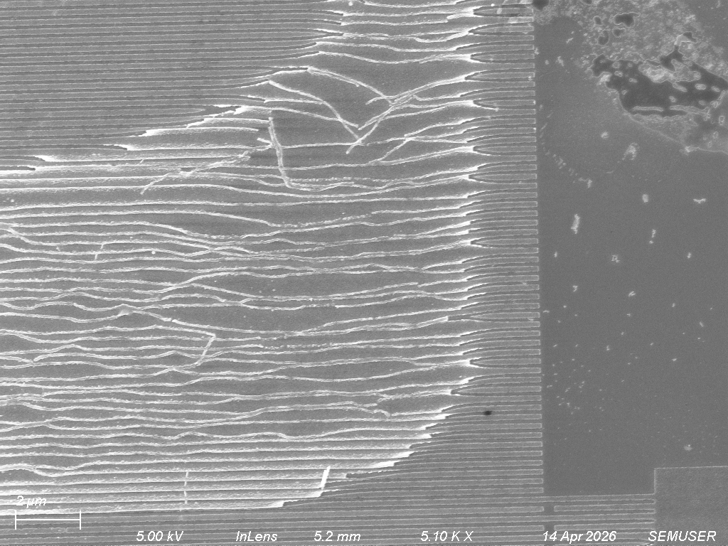
In overdosed devices, excessive exposure leads to energy spreading beyond intended regions, causing even gap areas to develop. The resulting metal strips are not fully attached to the substrate. Under SEM, the effect of not fully attached metal strips can be easily observed.
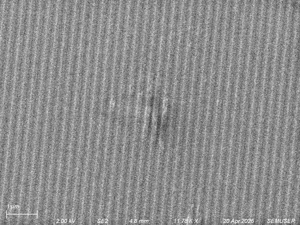
III. Contamination
During SEM imaging, contamination is present in the SEM image. Similar structures are also present in the AFM image. To further study the source of contamination, EDS was used to image a contaminated region. Due to the large interaction volume of LiNbO3, only very small beam voltages could be used, resulting in low X-ray signal. The EDS results did not reveal any useful information.

3. Discussion
GHz acoustic resonators were successfully fabricated using electron-beam lithography. The appropriate e-beam dose was determined by imaging devices fabricated under different doses using optical microscopy, SEM, and AFM. The metallic ratio of the fabricated devices aligns well with the designed ratio. Contamination present in both SEM and AFM measurements was analyzed using EDS but did not lead to a clear conclusion due to low X-ray generation.
Acknowledgments
The author would like to thank members of the Nichol Group for all of the resources and assistance, and Sean for support with SEM and EDS characterization.
References
1. Author A, Author B, "Title of paper," Journal Name, volume, page (year).
2. Author C, "Another reference title," Journal Name, volume, page (year).