Xiaoshu
Chen
| CONTENT | |||
| ABSTRACT |
ELECTRON
BEAM LITHOGRAPHY |
RESULTS & DISCUSSIONS | LAST
THOUGHTS |
|
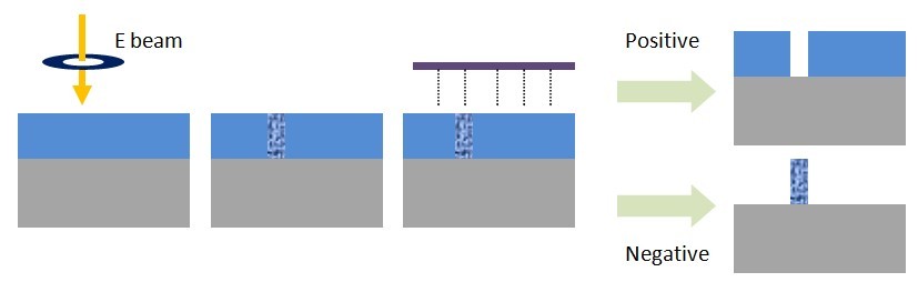
Eectron Beam Lithography (EBL) used in this project is converted from SEM (SUPRA 40VP FESEM of Institute of Optics at University of Rochester) EBL is a specialized technique for creating the extremely high resolution patterns. Comparing to the parallel light lithography, EBL is a serial lithography, and historically used to make photomask for light lithography. The electron beam scans across a surface covered with a resist film according to pre-written pattern and expose the resist, which is PMMA in this project. PMMA is a versatile polymeric material, and is one of the first materials developed for EBL. It provides high contrast and high resolution. After electron beam (e-beam) exposure, the large molecules of PMMA are break down to small molecules, which is more soluble than large molecules, so it is easier to wash away. This is called positive exposure. If PMMA is over exposed, it can change to negative e-beam resist, which is know as negative exposure. Large molecules get crosslink and form even larger molecules. Then the solubility of exposed area is smaller, and will be left after develop. When doing lithography, attention must be paid to the proximity effect. The proximity effect is the phenomenon that the exposure dose distributes and hence the developed pattern is wider than the scanned pattern. This is due to the interaction of the primary electrons beam with the PMMA and substrate. The typical procedures for EBL are showed in Figure 1 (Fig. 1). |
Fig. 1 Processes of electron beam lithography
|
Silicon
was chosen as substrate in this project, because silicon wafers are
relatively
cheap and they are semiconductor, then charging won’t be a
problem during
lithography. Before coating with resist, the silicon wafer was cleaned
by
methanol
in an ultrasonic cleaner to remove dirties and extraneous particles on
the
substrate. The PMMA used in this project was an anisole solution of 4%
(by
weight) PMMA (Solution A4) from MicroChem Corporation. The molecular
weight of
this
PMMA was 495K. A micropipette was used to measure the volume of PMMA to
be spun
on the spinning wafer. The spinning speed of the spin coating machine
was set at
3000 rpm’s for 90 seconds. According to the spin speed versus
film thickness
curves from MicroChem as shown in Fig. 2, the thickness of coated PMMA
is about 200nm.
After spin
coating, the wafer was hard-heated for 90 seconds, and then the
substrate was
ready for use.
|
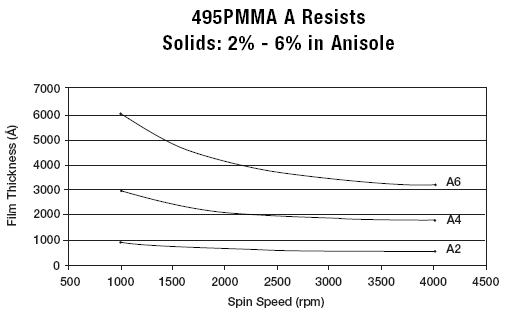
Fig. 2 The spin speed verus film thickness curves of PMMA
|
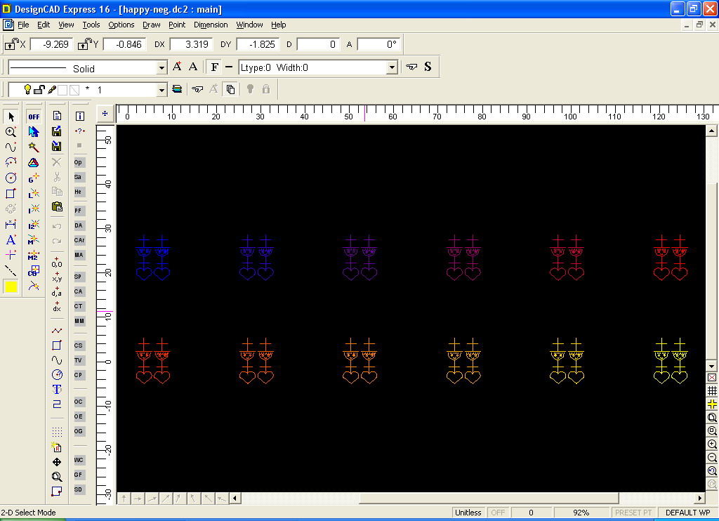
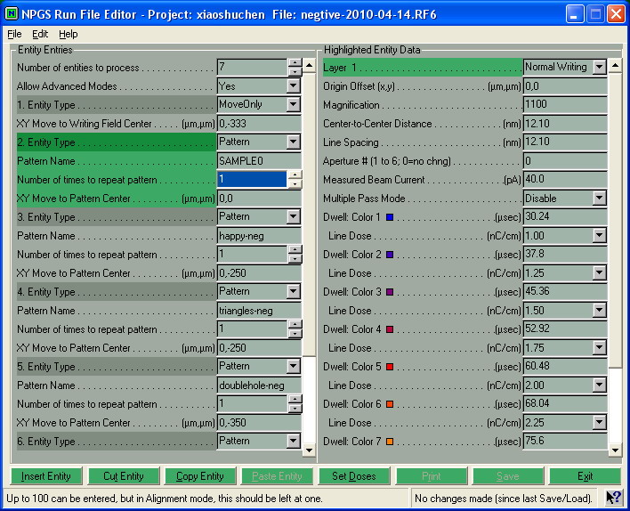
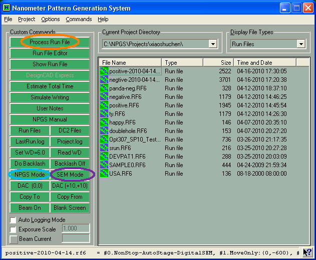
Nanometer Pattern Generation System (NPGS) is the top selling SEM lithography system at research institutions in North America, and it is becoming widespread around the world. NPGS is used to move the electron beam and determines the electron dose during exposure. Before doing lithography, patterns were created by software named DesignCAD Express 16, which is a comprehensive computer-aided design package that incorporates various drawing functions. The pattern is saved as .dc2 file (as shown in Fig. 3 ), and this file can be input into NPGS to make a run file (as shown in Fig. 4). Each run file contains one or more entities, and for each entity, the magnification, center-to-center and line-to-line distance, and electron dose are specified. Different colors are assigned with different electron doses. The center-to-center (line-to-line) distance is horizontal (vertical) distance between each exposure point. They should be small enough to get sharp corners and edges. |
|
First
the substrate was loaded into the SEM chamber
(making a mark before this step made finding pattern location
easier), and then the
chamber was
pump down to vacuum. To avoid exposure the sample at this
time, some gold nano particles were used as a calibration for beam
focusing and
astigmatism correction. And the beam current was measured by a
detector at
the sample stub. After this, the beam was turned off by turning on a
beam
blanker. Then moved the sample to locate the target area at
the beam
path. Set the SEM to external control mode by choosing the NPGS mode as
shown in
Fig. 5, and typed in beam current,
then processed the
run file(Process Run File) to write designed pattern on
the sample.
To drive PMMA to positive resist, the final beam aperture diameter is 10um. More electron doses are needed to drive the PMMA to be negative, so the final beam aperture is 30nm. And the accelerating voltage is 30KV in both cases to get high resolution. |
|
After
all patterns are written, the sample was sent to develop. Dipped
the substrate in developer
MIBK/IPA (3:1) for
40s, and then immersed it in another solution for 45s. Developing time
is
determined by the thickness of PMMA and also the concentration of
developer. Then light
microscope were used to find the position of the pattern on the
substrate for easier observation in SEM.
|
|
To get better images in SEM, a sputtering coater was used to coat the sample with 3nm gold. Gold film makes the sample more conductive and easier for surface inspection. Thickness of coating film is determined by the roughness of sample. Sample with rougher surface will demand thicker coating. And the thickness of fiml is controlled by coating time and current. |