Fig. 6 SEM image of positive exposed PMMA nanorods.
Xiaoshu
Chen
| CONTENT | |||
| ABSTRACT |
ELECTRON
BEAM LITHOGRAPHY |
RESULTS & DISCUSSIONS | LAST
THOUGHTS |
|
The coated patterns were observed both by SEM and AFM. Followings are resulting images and discussions. |
|
The inlens detection mode of SEM was
used for pattern
observation. In this mode, the Auger electrons are detected. As Auger
electrons come from within about 10nm below the surface, this
mode
mainly provides surface structure information.
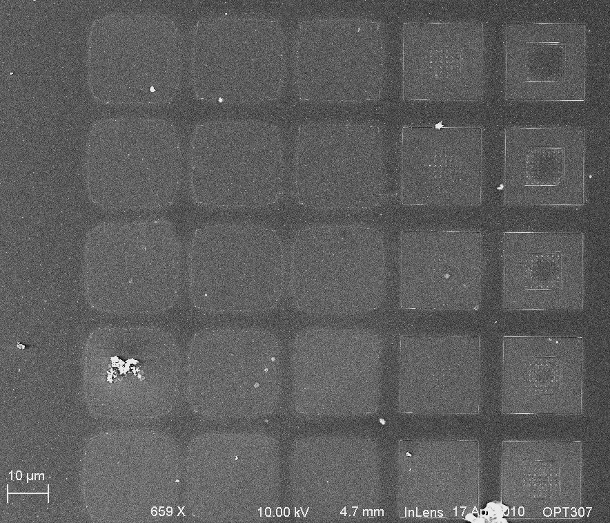
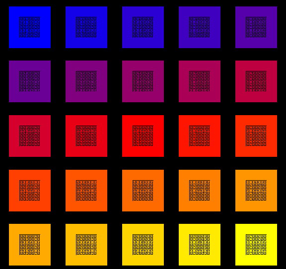
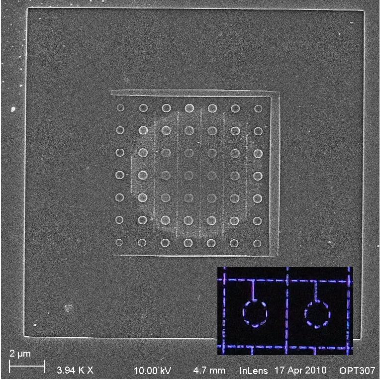
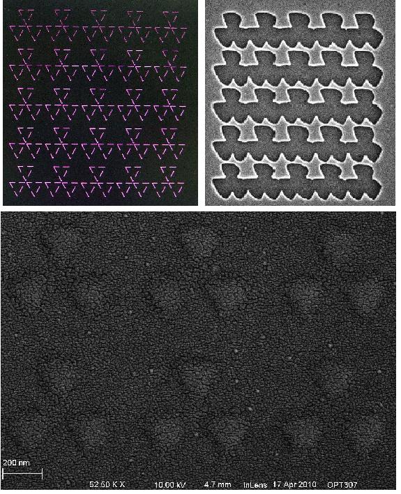
Fig. 6 is the image of positive exposed PMMA
nanorods. The
pattern is
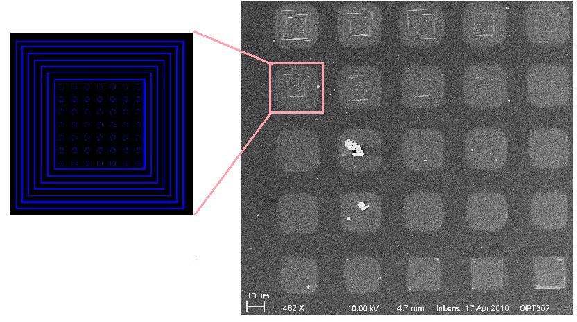
shown at the right. Every small square in the SEM image corresponds to
a colored square in the pattern. And different colors denotes
different
electron dose. This method is used to find the right
dose for a
pattern. It can be seen that the doses for columns one to four are too
large for driving PMMA to positive and not enough for driving it to
negative for this pattern. So after developing, the exposed PMMA were
washed away. The doses for center areas of first and second square in
column
five are good for this patterns
as shown in Fig. 7(a) and (b).
The fine
lines among nanorods if
Fig. 7 (b) is because those areas were exposed twice due to the
proximity effect (see enlarged picture for center area in the insert of
Fig. 7(b)), so the PMMA became
negative and left after develop. The square edge round the pattern in Fig. 7 is
unexposed PMMA, and it can be moved away with acetone.
|
|
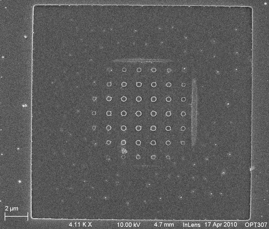
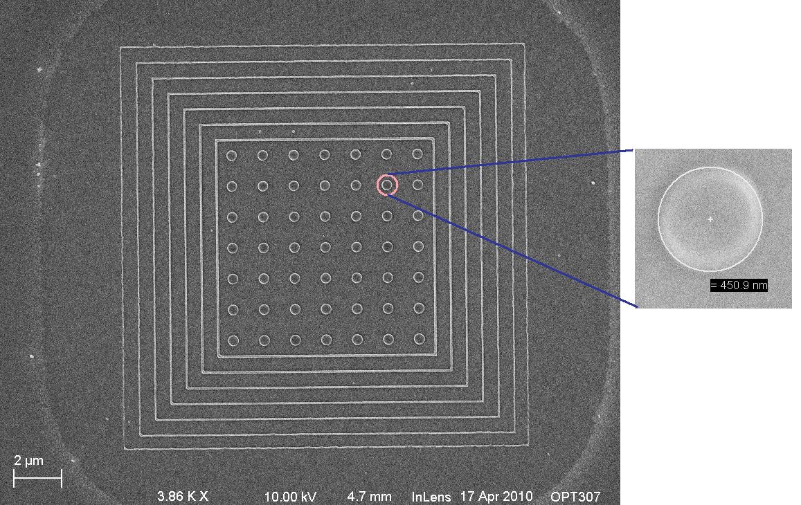
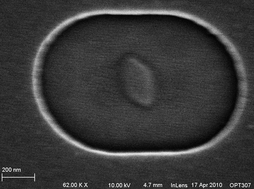
Fig. 8 is the image for negative driving PMMA nanorods. Compare the insert of Fig. 7(b) and Fig.8 , it can be seen that to get PMMA nanorods, the areas around the circles need to be exposed in positive case, while in negative case, we need to expose the circles. Fig. 8 shows that most patterns were not enough exposed, and after develop, the PMMA was washed away. The dose for this first row in Fig. 8 seems good. Shown in Fig. 9 is the detail of first pattern in Fig. 8. The pattern was accurately transferred to the PMMA, except the outmost square mirror seems thinner than inner square mirrors, as shown in Fig . 10. The diameter of the circle was designed to be 500nm which is larger than the diameter of actual nanorods, which suggests that the pattern were not enough exposed. |
|
Fig.
11(top-left) is pattern for driving PMMA to
form triangles. Each side of triangle is 300nm in the pattern, and
distance between each triangle is 30nm. The electron beam
is supposed to drive the PMMA in the triangle area to negative
according to the pattern design. Fig. 11
(top-right) is
the SEM image for PMMA insufficient exposed, so the PMMA in the
triangle area became positive and has been washed away after develop.
The electron dose in Fig.
11 (bottom) should be enough. The blur corners
and edges is because that the
center-to-center and line-to-line distances are comparable to the
length of the patten. And the wider distance than design suggested that
this pattern was not enough exposed.
|
|
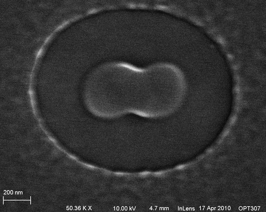
Fig.
12 (top) is overlap double circles that designed to drive the
area of circles to be exposed and drive the PMMA to negative. It can be
seen from Fig. 12 (bottom-left) that the doses for the two circles were
not enough, the
overlap area was exposed twice and drove PMMA to negative. And the does
in Fig. 12
(bottom-right) is enough. Smaller
center-to-center and
line-to-line distance would make the edge sharper.
|
|
Followings are SEM images for irregular shapes by
electron
beam
lithography.
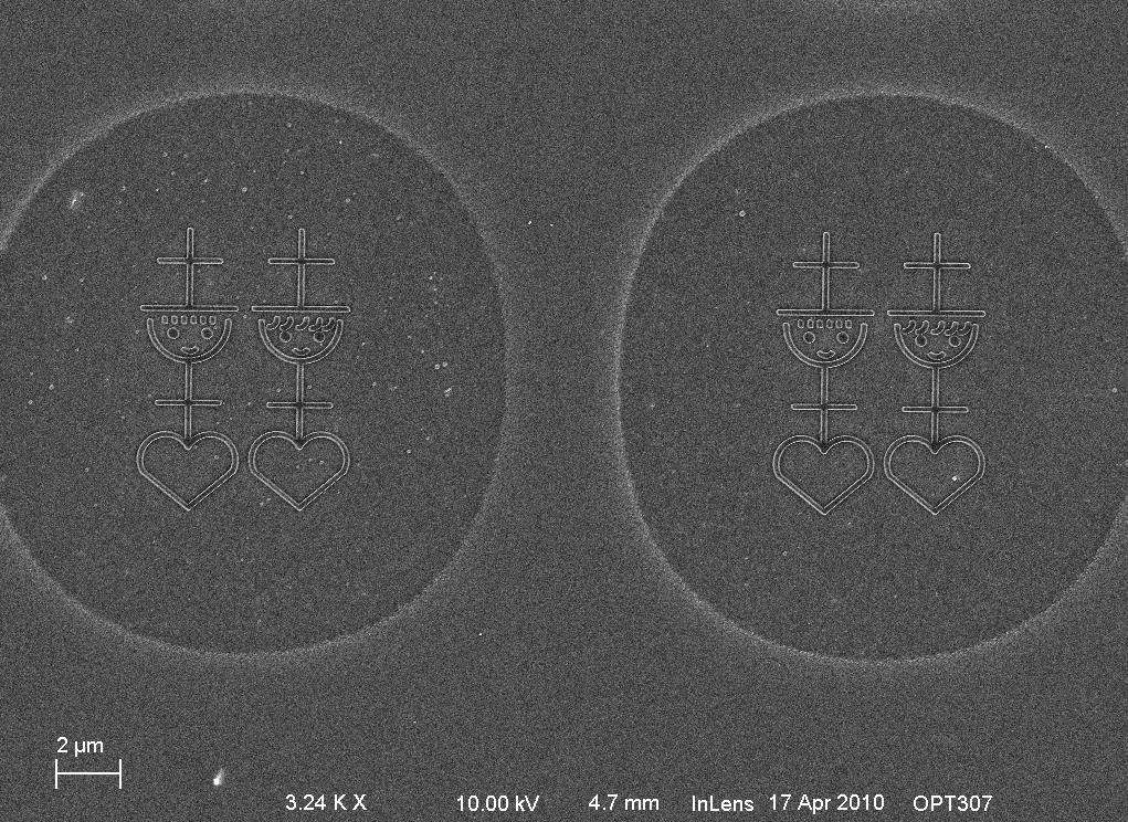
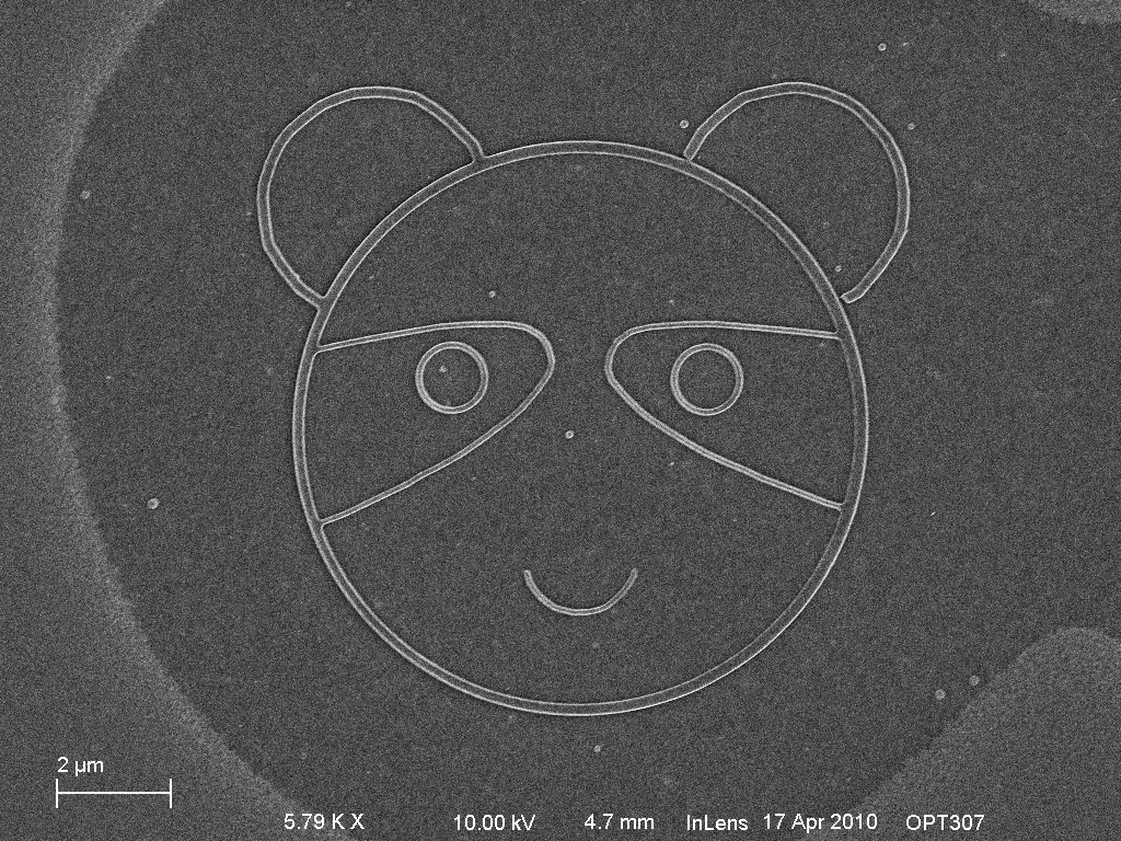
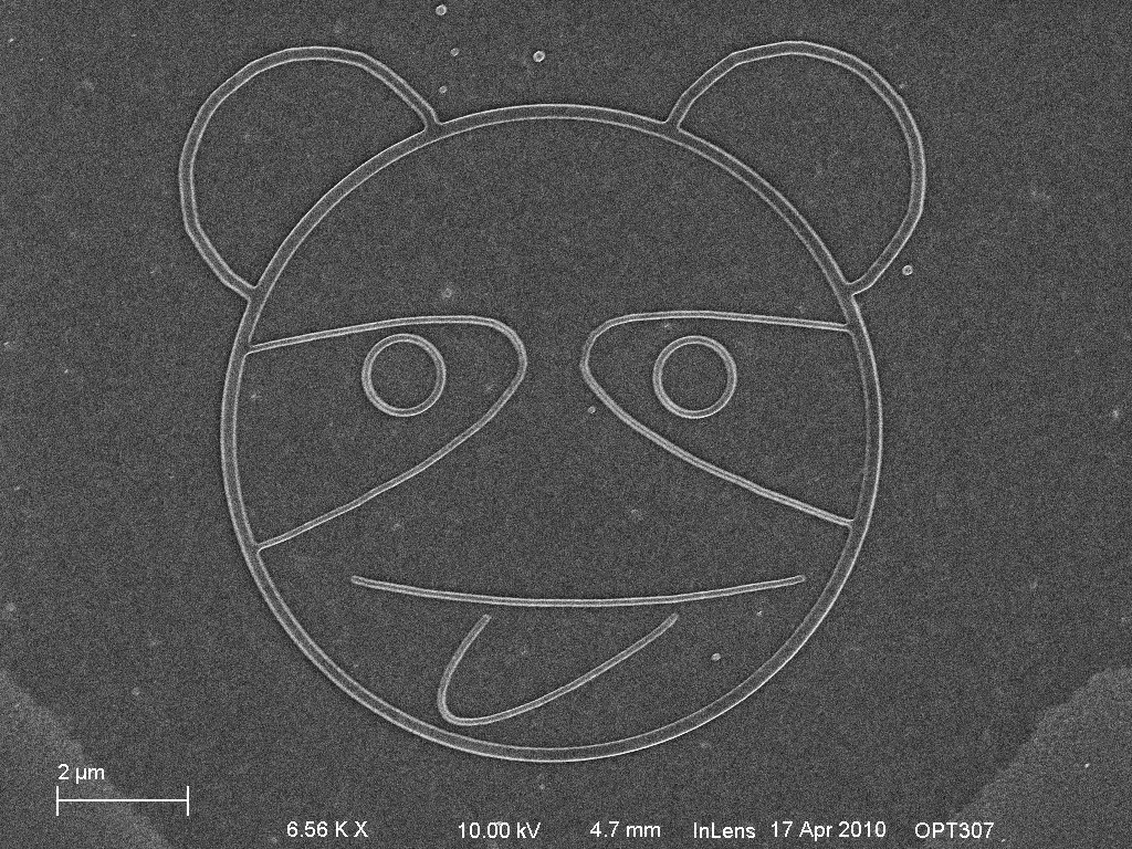
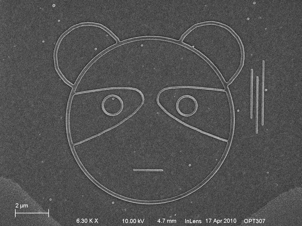
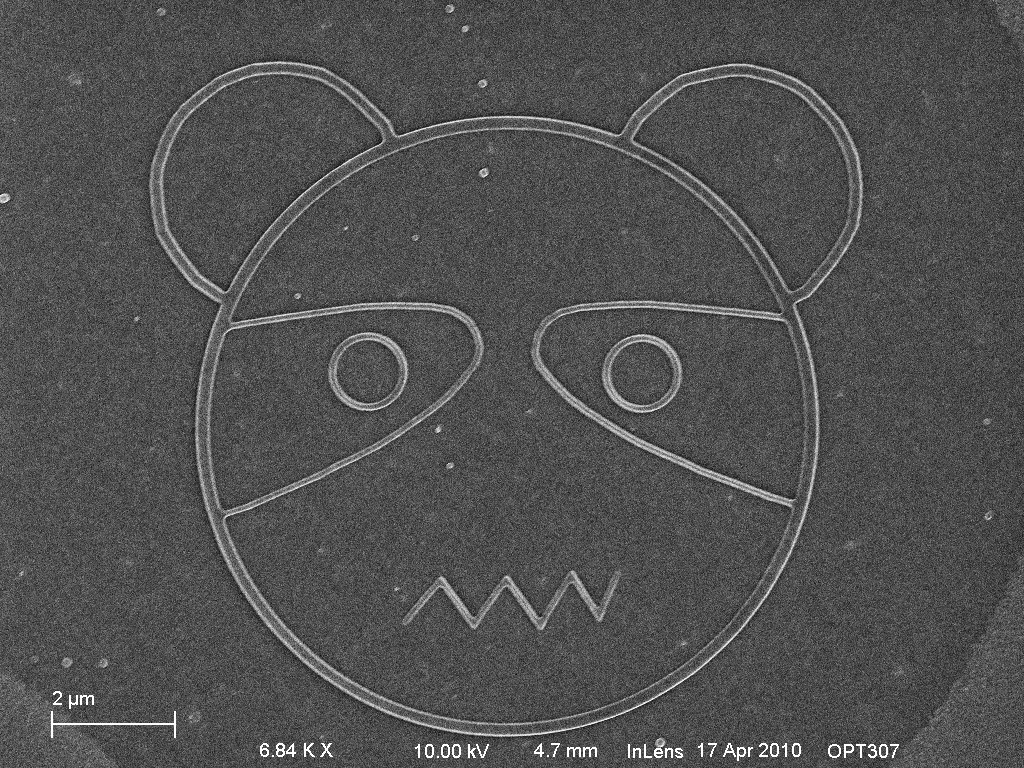
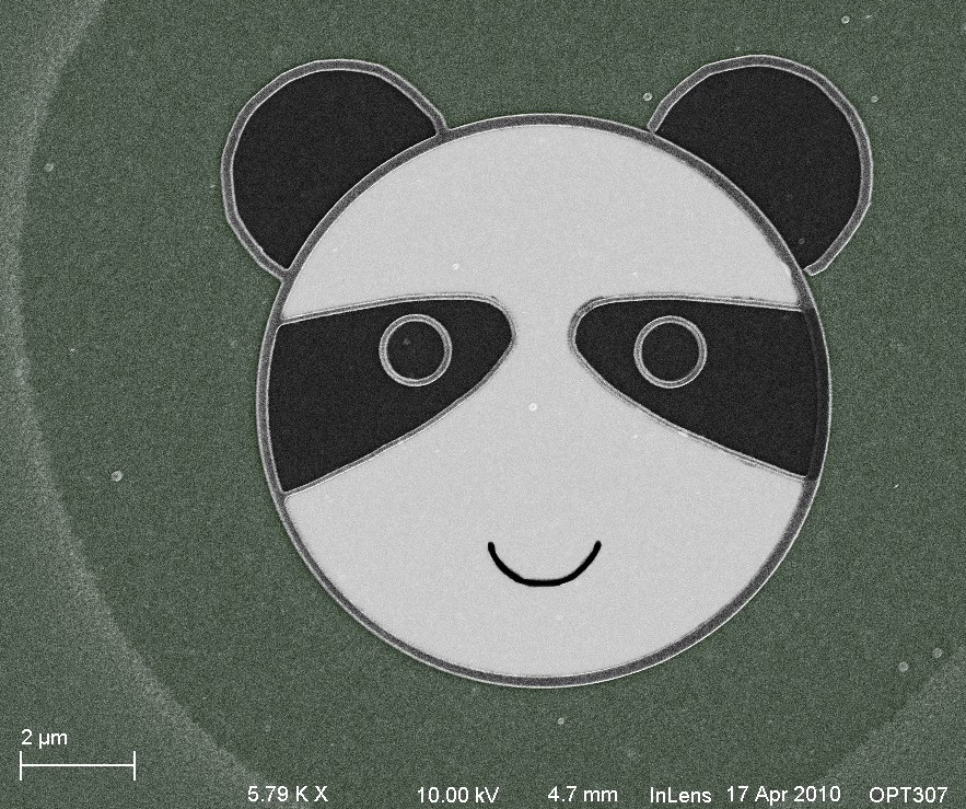
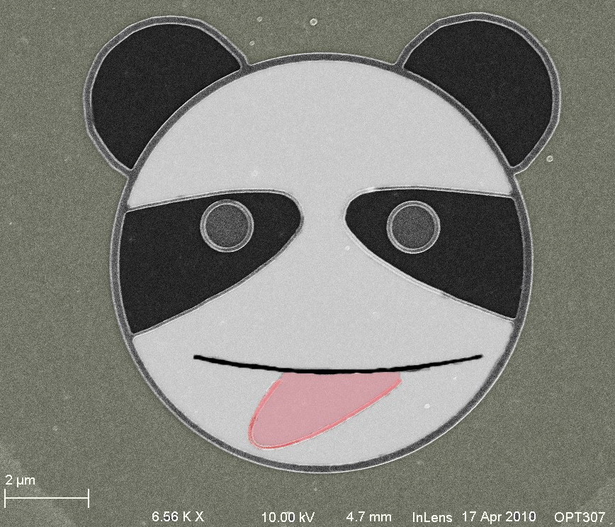
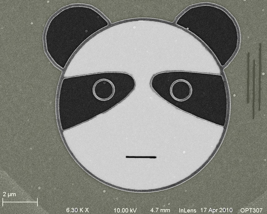
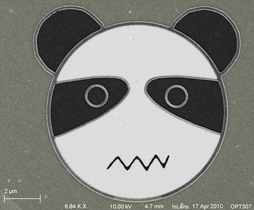
Fig. 13 shows popular Chinese panda facial expression. The line
to form the
panda is 100nm. The first expression is a lovely and quiet smile means
happy. The
second
panda is smiley with its tongue out
impishly. The third
panda is saying: Oh my god. You did this? Though I feel pity, I have
nothing to say. The fourth panda is unhappy or feel it is difficult to
do something, for
example: Oh, so many deadlines~~~ . And the PMMA vacancy in these SEM
images are colorized as shown
in Fig. 14. As the SEM images are grayscale pictures,
reasonable colorization will provide more information.
|
|
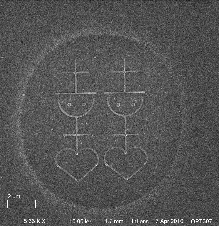
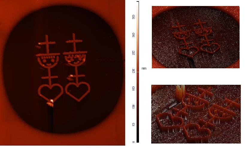
Fig. 15 (top-left) is the Chinese traditional marriage totem--red double happiness. At the wedding, Chinese people stick these totems on the windows and furnitures to bless the newly-married couple love and happy in their new life. Also see Fig. 3 for the double happiness pattern, they are designed to drive the lines to be negative and the width of the line is 100nm. Fig. 15 (top-right ) shown that the husband's and wife's hairs were not sufficient exposed. Fig. 15 (bottom) are well exposed double happiness. The proximity effect is very obvious here. It can be seen that the PMMA adjacent the double happiness were driven to positive and left a circle PMMA vacancy after develop. |

|
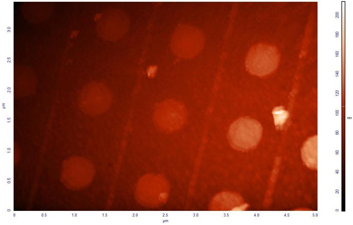
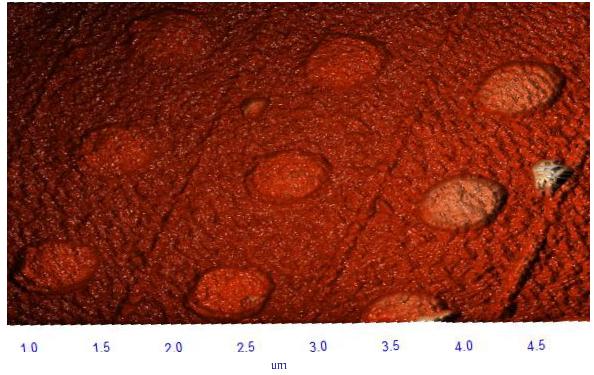
AFM is a mode of scanning probe microscopy, and it
works on the van der Waals force between the tip and sample surface
atoms. In AFM, the tip is mounted
on a
reflective cantilever. And the back of cantilever is coated with gold
or other
reflecting materials. The tip scanned the sample surface line by
line (raster scan). Then a laser beam will sense the deflection of
the cantilever,
and the signal is detected by a position sensitive quad diode
detector. The AFM used in this project is Solver Next from ND-MDT
Company. The resolution of of AFM is dertermined by the radius of the
tip (20-50nm in this project) and scan speed (the slower the speed, the
higher the resolution). Compare to SEM, the main advantage of AFM
in this
project
is that it provides accurate measurement in three dimensions. Fig. 15
is
the 2D
version of AFM scan of the positive exposed PMMA nanorods. The
color
reveals the height is in nanometer scale. And Fig. 16 is 3D version of
the
same area. |
| Electron Flight Simulation software was used to simulate a visual representation of how the primary electron beam interacts with PMMA film on silicon substrate. It utilizes Monte Carlo method to calculate the interaction of electron beam and sample. Fig. 18 is the sample conditions with 200nm thickness PMMA film on silicon substrate. The chemical formular and density of PMMA can be added to the database for calculation. And the accelerating voltage was set to 30KV. Then run the simulation to get the interaction volume of of electron beam and sample as shown in Fig. 19. The red line is electron beam, and horizontal gray line is PMMA layer, below which the white area is the silicon substrate. The blue zone is the interaction volume. It can be seen that though the beam diameter is nano meters scale, the actual distribution of electrons is about 12 mircos wide according to the simulation. The simulation results show how proximity effect happens. It can be imaged that adjacent exposure dots will affect each other if they are close enough. |
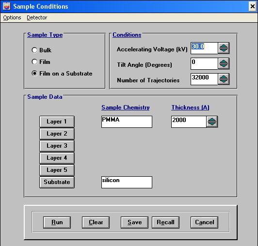
Fig. 18 The panel of the Electron Flight Simulation Software and sample condition that needed for simulation.
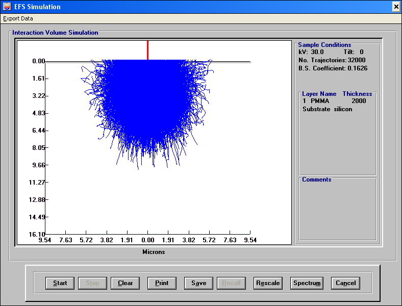
Fig. 19 Simulation result of electrons interact with 200nm thick PMMA film on silicon substrate.