The transmission electron microscope, or TEM for short, can be used to look at a very thin sample by shining electrons through it, just as you would look at a transparency or piece of film by shining light through it. In addition to looking at the transmitted image, it's possible to use electron diffraction to image the crystal structure of very small samples. By measuring the diffraction pattern, we can tell something about the crystal structure.
The goal of this TEM work was to look for evidence of what phases were present in the sample of PMN-PT. Because the sample had (nominally) 29% PT, it fell into a range where the exact phase composition is unknown, although the presence of a rhombohedral or monoclinic structure is suggested by current literature. I hoped to find evidence supporting some kind of phase composition.
The sample was a single crystal of unpoled PMN-PT, which had been polished down to a thickness of about 10 microns. Even at the very high accelerating voltage of the TEM (200 KeV), this is much too thick to be transparent. This was illustrated by an electron flight path simulation.
However, during polishing a corner of the sample was broken off, leaving a chipped edge. I hoped to find an edge region thin enough to be transparent, and I found several such regions. Using darkfield illumination I was able to identify areas showing diffraction, and I took diffraction patterns from some of those regions.
Imaging this sample was tricky because the piezoelectric material reacted to the high-voltage electron beam by expanding and contracting in the beam. Thus, moving the sample or changing the beam focus, alignment, or intensity all caused the sample to move. This made the focusing and astigmatism correction processes even more iterative than usual, since every adjustment caused the sample to shift itself.
In addition, apparently the high voltage of the electron beam induced such a high ferroelectric strain in the crystal that the crystal actually broke. Pieces literally and visibly popped off of the crystal as it was panned under the electron beam. To minimize this effect, extra care was required to keep the beam less focused and intense. Breakage of the crystal also seemed to decrease the number of good diffraction sites.
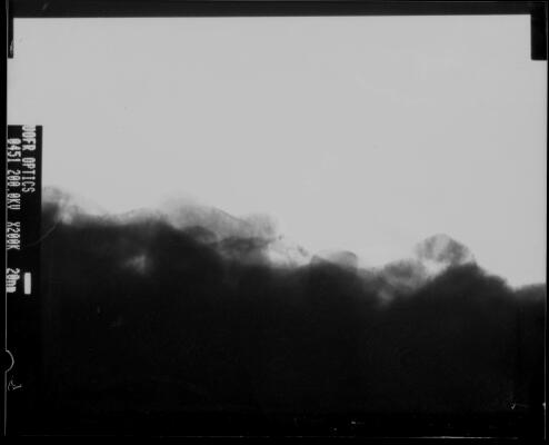
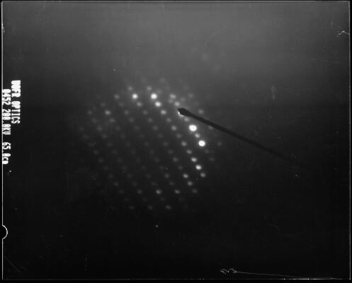
Here are three pairs of pictures. Each pair contains an area-limited diffraction image, and a brightfield picture of the area from which the diffraction image came.
Figure 1
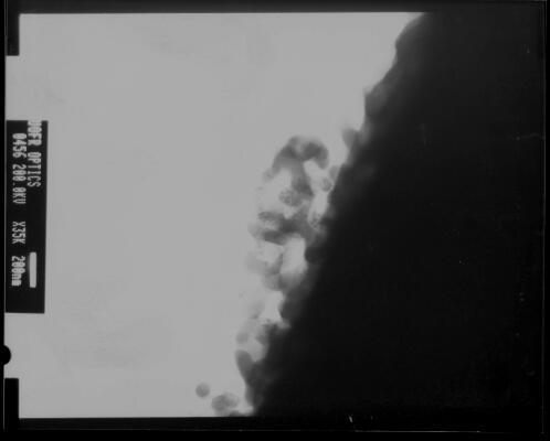
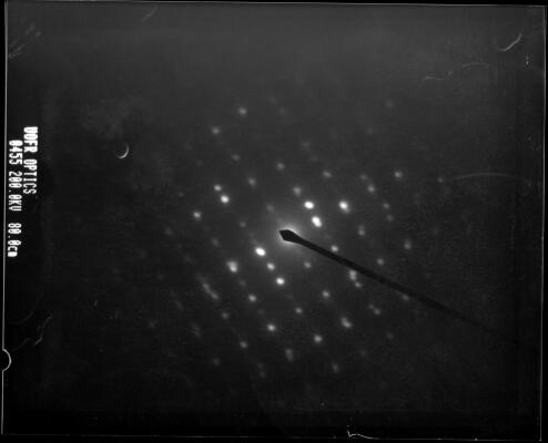
Figure 2
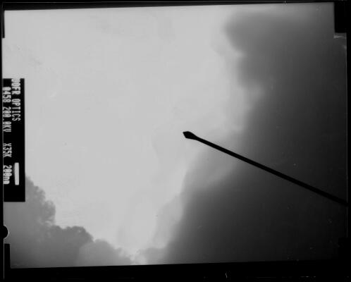
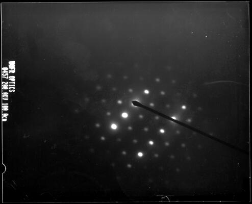
Figure 3
The lower left corner of the last darkfield image shows the edge of one square of the sample holder's copper grid. It was included to demonstrate the difference in appearance between the copper grid and the sample.
These pictures make one thing very clear: the sample consists of crystallites with different orientations relative to the beam. This is obvious from the differences between diffraction patterns: one is rectangular, one is nearly square, and one is hexagonal. The different spacings and relative angles of the dot lines in each case clearly show that different planes are being imaged in each case. This could be caused by different domain orientations in the crystal (similar to twinning), or possibly the imaged regions are loose pieces that were re-oriented. It's not immediately clear, however, if these are different phases.
The diffraction patterns in the right-hand images can be measured in order to calculate the spacing of the lattice planes for each picture, using the simple formula R*d = λ * L, where d is the spacing of lattice planes, L is the camera length, λ is the wavelength of the electrons, and d is the physical spacing measured on the picture itself. The results are:
Several researchers have measured the lattice parameters of PMN-PT at different compositions (for example, see Ye, Noheda, et. al. in Phys. Rev. B 64 p184114) and found pseudo-cubic lattice parameters of around 4.01-4.05 A. This suggests that the result in Figure 3 may be a PMN-PT diffraction pattern.
However, given this lattice constant, it seems unlikely that the other two patterns are PMN-PT unless the calculation is completely mistaken or overrun with error. Interestingly, the lattice constant of copper is known to be about 3.61 A, close enough to suggest that perhaps the first two results are the result of some kind of vacuum deposition or sputtering process. In particular, the brightfield image in Figure 2 suggests a rather lacy extended structure which might be a probable result of copper recrystallization.