This section of the project was the primary focus. The goal was to use the SEM to observe domain patterns at the surface of a piece of PMN-PT, and then to verify those domains by observing the relief-polished surface with a DIC optical microscope.
This was the most challenging part of the project. Initial sample scans showed very little detail at all, and different sample mounting methods were tried and discarded before the working method was found.
In order to see domains with the electron microscope, it was necessary to have the domains exhibit their ferroelectric behavior. In order to achieve this a poled sample was used, and a voltage was applied along the poling direction to induce a contraction in the material, which in turn induced regions of positive and negative charge on the sample surface coinciding with "up" and "down" domain regions. These positive and negative regions acted to attract or deflect the electron beam, respectively resulting in darker or lighter splotches.
In order to remove any possibility of mistake, the sample was not relief polished before the SEM test. Instead, the sample was polished down to a 1 micron grit, which is the last polishing stage before relief polishing. In this state there are no relief patterns and the surface of the sample is covered with scratches from the 1 micron grit. Steve Robinson, our lab technician and polishing expert, prepared the sample to my specifications.
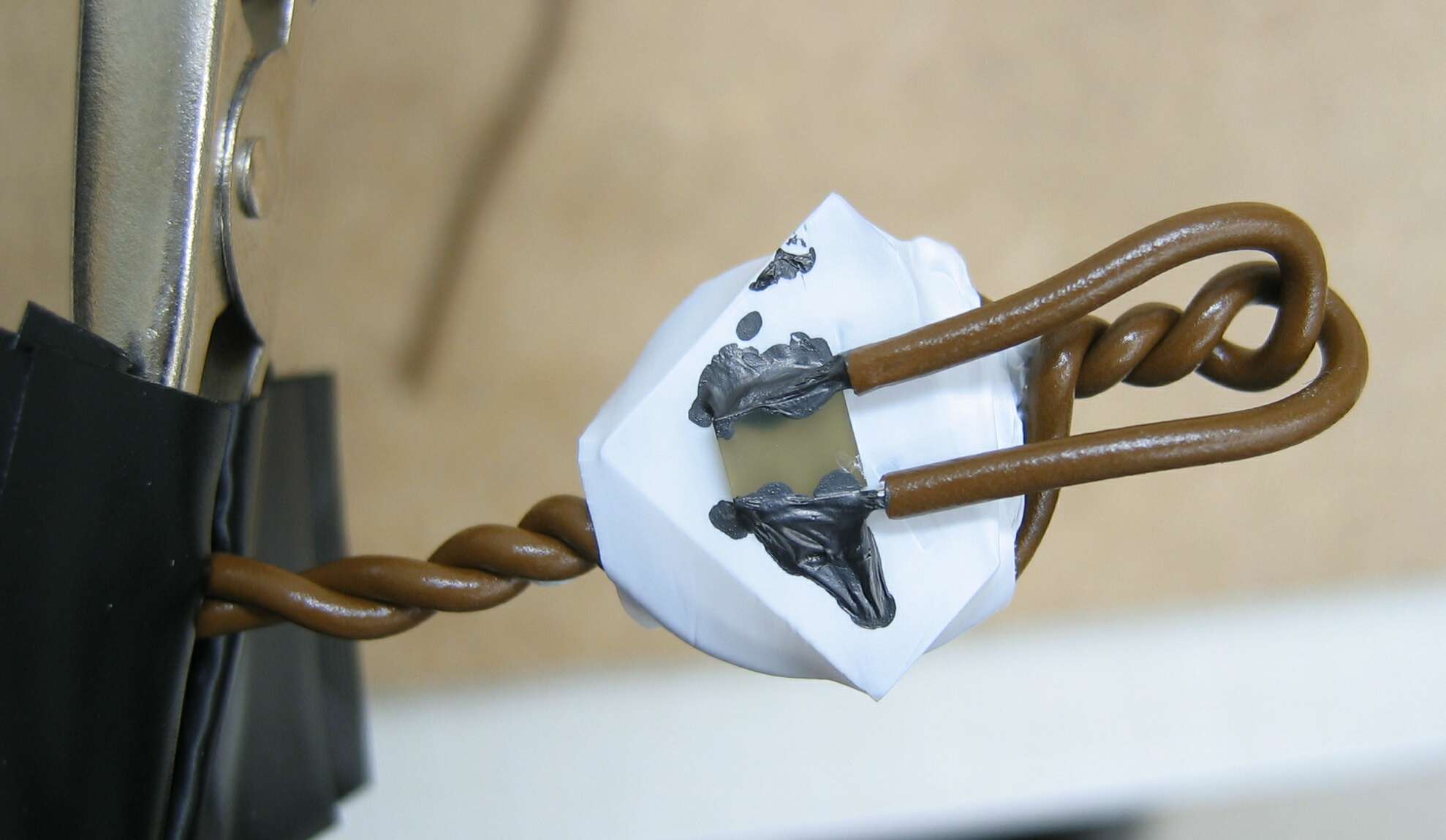
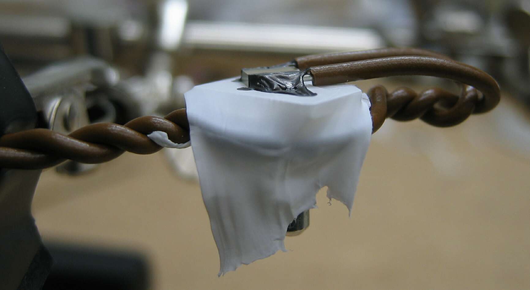
In order to apply a voltage across the sample it was vitally important that the sample be isolated from the sample stub, and that each side of the sample be electrically isolated from the other side. To achieve this the stub was covered with several layers of teflon tape, then a small piece of microscope slide glass was placed on top, followed by another later of teflon tape. The electrical wires were twisted around the stub rim for stability, to prevent flexion of the contact points on either side of the sample. The sample was pinned between two bare wire ends and lightly attached with some conductive graphite glue. The final result looked like this:
The sample was left uncoated, because the only way to observe the domains was to allow them to build up a charge. Any kind of conductive coating would have prevented that. Obviously, this limited and drastically reduced the quality of the final images.
The sample was placed in the SEM and pumped down. For the experiment the accelerating voltage was set at 1 kV, both to minimize the amount of charging and to maximize the chance of deflection by the domain charges. The sample was connected (through a vacuum feedthrough) to a high-voltage (0-400V) power supply. One side of the sample was maintained at power supply ground (and through it to building ground), and the other was varied from 0 to -300V.
Here is how the sample looked as it was charged from 0 to -300V. These pictures were all taken with the chamber SE detector. At higher voltages image quality decreased even further because the voltage applied to the sample caused massive beam astigmatism.

0 V, 80 V, 160 V applied to sample.
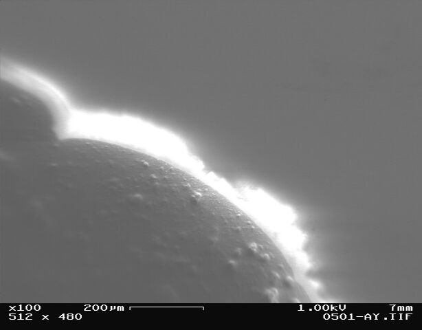
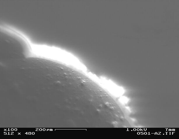
240 V, 300 V applied to sample.
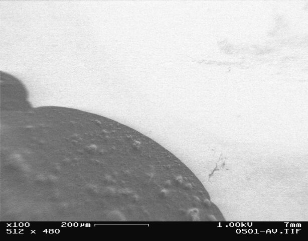
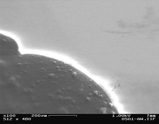
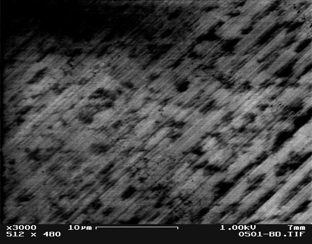
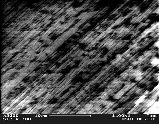
The rounded dark area in the lower left half of the picture is part of the carbon glue on the top of the sample. The very narrow bright region around it is the extent of the high-voltage region. Within this region I was able to find domain-like structures. Here are two pictures of close regions in this area, the first with 0 V applied and the second (contrast-enhanced) with 300V applied.
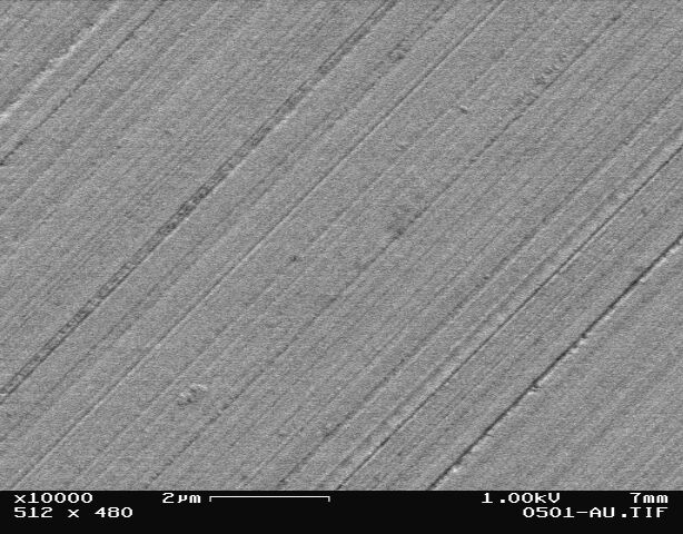
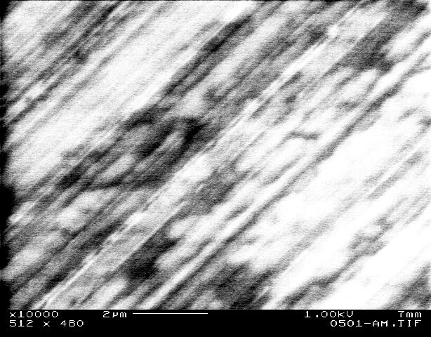
Although polishing scratches are visible in both, there is clearly a dark-and-light mottled pattern showing in the lower image. Interestingly, the in-lens detector showed very little detail in either case, and was generally not useful during this project. The chamber detector seemed much more sensitive to surface features and surface contamination.
After spending any amount of time on a particular region, the "domain" patterns seemed to quickly diminish. Because of this, I developed the technique of focusing in a nearby area, shifting quickly to a new location, and immediately starting a single slow scan. The following two images (slightly contrast-enhanced) were taken this way with 300 V across the sample.
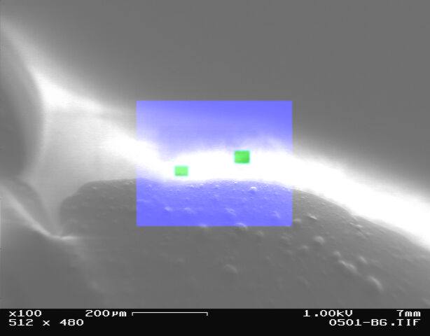
In order to locate these regions with the optical microscope, I took several wide-angle pictures to localize them. The following image has two contamination squares in those locations, which have been slightly colorized to emphasize them:
Finally, the sample was demounted, relief polished, and inspected using a light microscope in DIC (Differential Interference Contrast) mode. The same region above can be seen below:
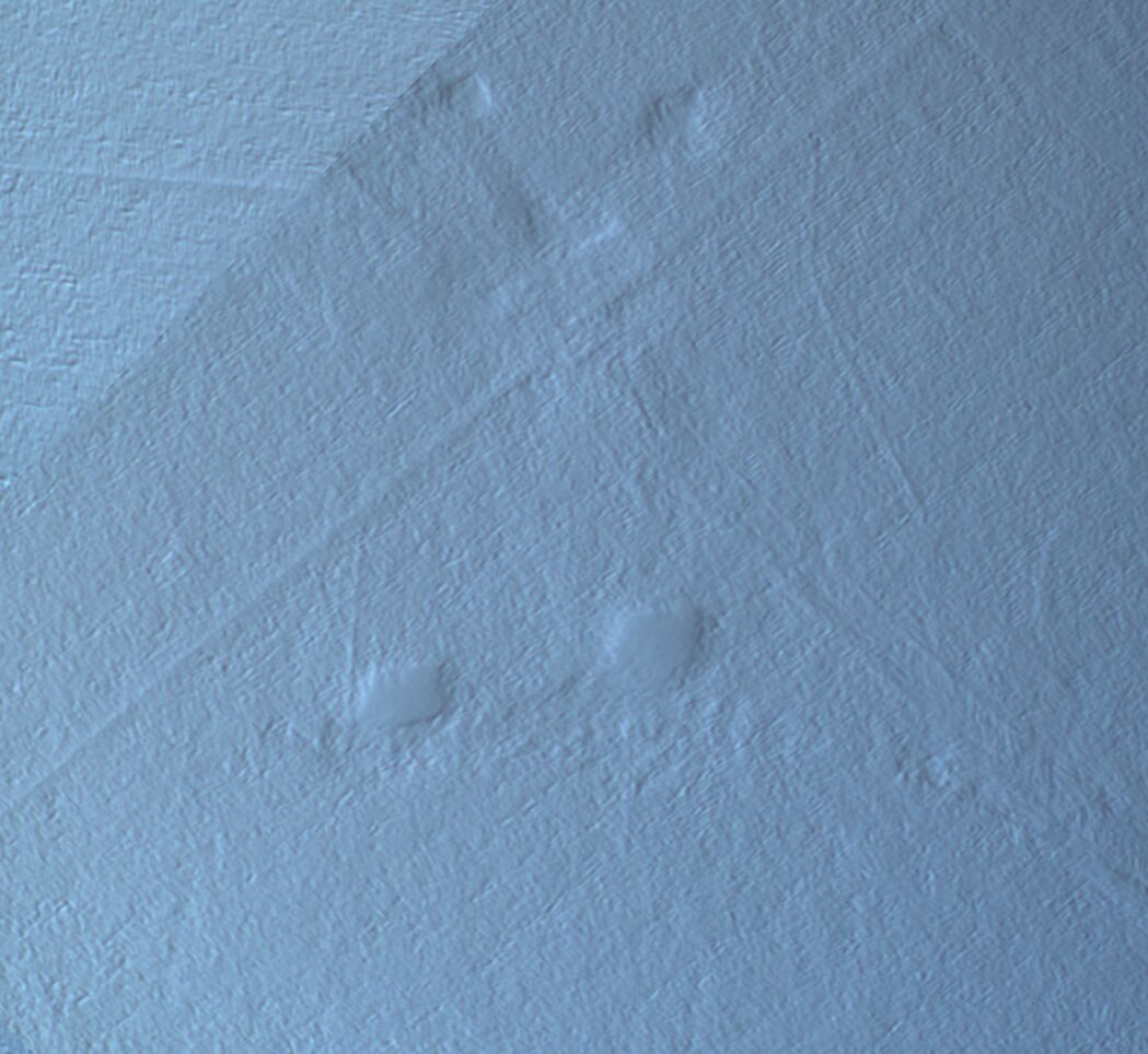
Surprisingly, there is no domain structure visible in those areas because the electron beam in the SEM re-poled the domains! On reflection, this is a perfectly obvious event, because the high voltage of the electron beam is localized to a very small area when it scans, and it's only natural that a high potential localized on the surface would cause poling effects.
So the goal of this project is fulfilled, although not in the way I'd originally hoped. It seems very definite that the mechanical etching/relief polishing process does reveal domains, because the SEM created some and they were revealed. However, it's very difficult to tell whether the above images really do represent imaging of domains by the SEM. Only further experiments will reveal the answer to that!