| OPT 407 Course Project | Zhimin Shi, April 2006 |
 |
Microscopic Study on Artificial Metal-Semiconductor Nano-Materials |
|
Particle size analysis
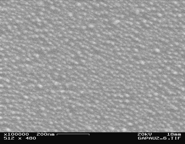
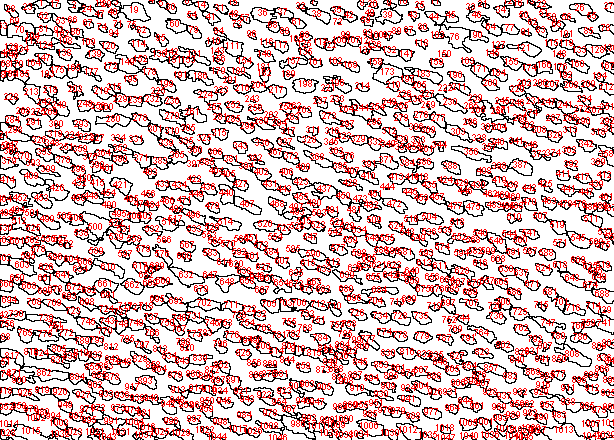
Fig. 5.1upper: SE image of sample #6 (Au nano particles on bulk GaP); bottom: outline of nano particles obtained using ImageJ.
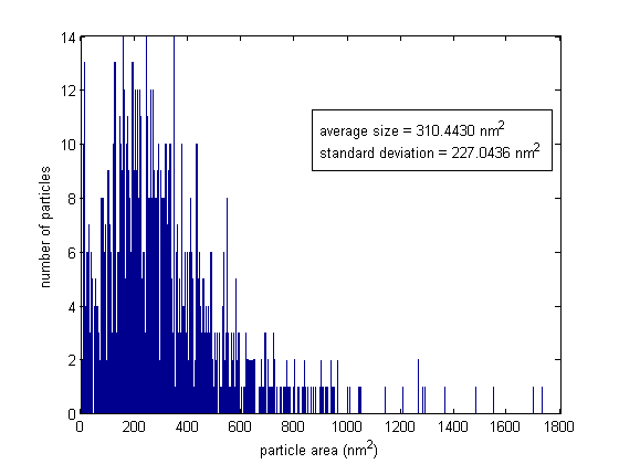
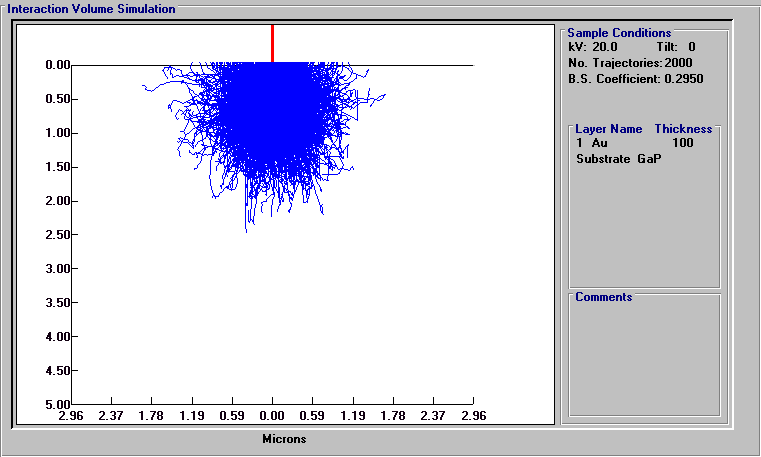
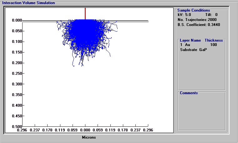
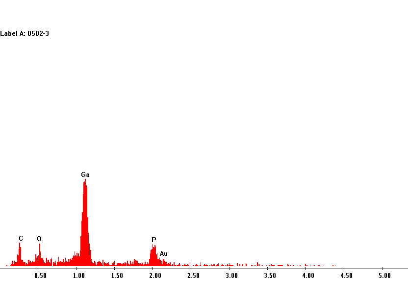
Fig. 5.2 Histogram of the particle size distribution of sample #6. It has been shown previously that the X-ray signals from gold are missing in the X-ray spectrum of sample #4. It was also noted that none of the nano-particles are clearly observed using backscattered electron signal. There are a few reasons to explain this missing line. First of all, the size and the volume of the nano-particles are in the scale of tens of nanometers. The interaction volume of the electron beam is, however, much larger. The upper plot of Fig. 5.3 shows the simulated interaction volume of a 20 keV electron beam incident on a 10nm thick gold film on GaP substrate. One sees that the interaction volume is in the order of microns, which is much larger than the dimension of the gold nano-particles. Meanwhile, one knows that X-ray signals are typically produced when a primary electron causes the ejection of an inner shell electron from the sample and an outer shell electron takes its place while releasing some energy in terms of X-ray. This indicates that X-ray signals are usually generated at the bottom part of the interaction volume, and in our samples there is no gold beneath the substrate in that region. An alternative solution to observe the gold M line is to use a lower electron energy, i.e., to use a smaller interaction volume. As shown in the bottom plot of Fig. 5.3, the interaction volume is much smaller (in the order of 100 nm ) when the accelerating voltage is only 5kV. To make sure this will work, X-ray spectrum are obtained using numerical simulation and experiment on sample #4. Fig. 5.4 shows the experimental result, which is quite consitent with the numerical calculation.The gold peak is barely observable in this case, which is limited by noise of the signals.
. Fig. 5.3 Interaction volume with upper: 20keV; bottom: 5keV electron beam incident on 10nm thick gold film on GaP substrate. Fig. 5.4 X-ray spectrum for sample #4 (Au nano-particles on bulk InP) with accelerating voltage of 5keV
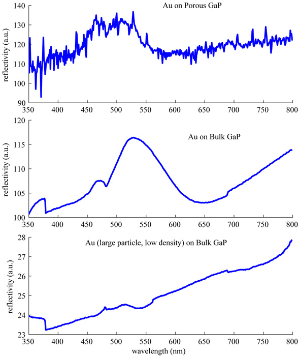
Interpretation of Optical Property of samples The optical property of the artificial nano-materials are dependent on the size and density of the nano-particles. Fig. 5.5 shows the reflectivity measured at different wavelength for samples #6, #4 and #5. One clearly sees that an plasmon resonance occures between 550 and 650 nm for samples #4 and #6. This resonance is largely determined by the size of the gold nano-particle because plasmon resonance is related to metals. Sample #5 have much larger gold size and very small particle density, and therefore it does not show such resonance. Similar procedure can be made between SEM particle analysis and optical property measurement to determine more accurately the relation between nano-structures and their optical property.
Fig. 5.5 Measured Optical Reflectivity as a function of wavelength for (from top to bottom): #6: Au on porous GaP; #4: Au on bulk GaP; #5: Au (larger size and low density) on bulk GaP.
|