| OPT 407 Course Project | Zhimin Shi, April 2006 |
 |
Microscopic Study on Artificial Metal-Semiconductor Nano-Materials |
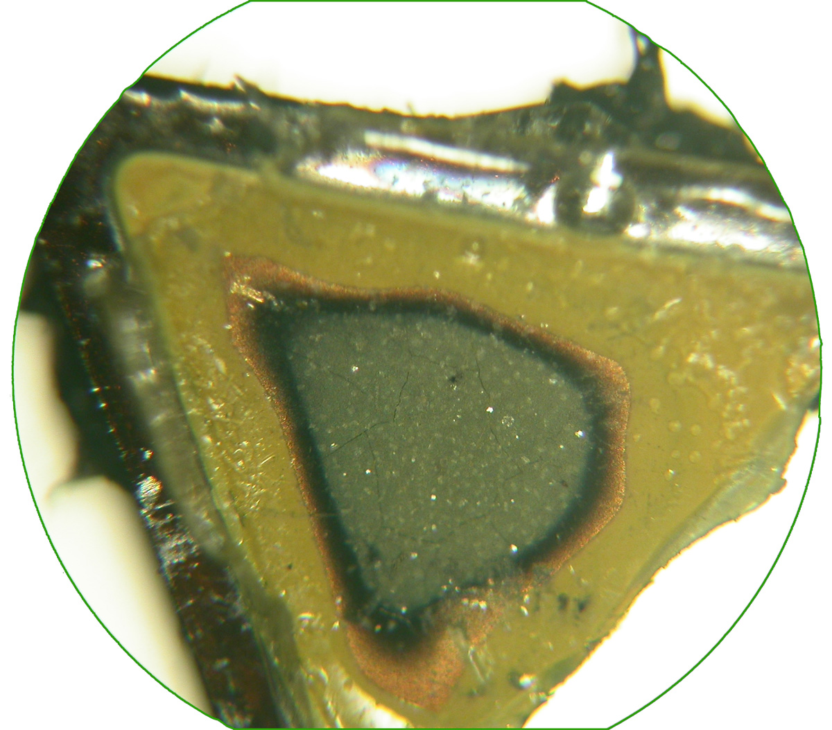
A light microscopy photo of a sample (#6: Au nano particles on Porous GaP): There are four colors from out to center, namely, dark-transparent, yellow, reddish-golden, and grey. These color corresponds to bulk GaP, porous GaP, gold film and gold nano-particles deposited on porous GaP, respectively. |
The properties of nano-composites are often dramatically different from those of bulk constituent materials with identical chemical composition. For example, Porous III-V semiconductors offer a potentially attractive alternative to bulk semiconductors as a nonlinear medium exhibiting a strongly enhanced nonlinear electrical and optical response[1], [2]. Thus, fabricating and studying such materials has attracted a great amount of attention in recently years. In particular, researchers have developed a novel technology for doping of nano-structured semiconductors by metals. The technology is based on AC electrochemical deposition under various conditions. Using this technology, metal or rare earth (Eu, Er, Ag, Cu, Au, Pt) nano-clusters are successfully deposited on the internal surface of disordered porous GaP and InP. Under certain conditions, metal nano-tubes were formed in highly ordered nano-structured InP membranes. Microscopic study of these nano-structured composite materials is one of the means that are necessary to examine the result of fabrication. The imaging on the cross-section of the porous nano-structures would help to understand the kinetics in the formation of the structures, which would help improve the fabrication process. Measurement of the sizes of the pores and the thickness of the metal films would offer important parameters for accurate numerical modeling and prediction of their properties. Furthermore, due to the nano-scale dimension of the structures and the combination of metal and semiconductors, it also poses a challenge for microscopic observation. This project would offer a direct measurement for various samples fabricated under different conditions, and would offer important statistical numbers on the dimensions of the structures which are important for analysis and prediction of the material’s property.
References: [1] A. I. Dikusar, et. al., “Kinetics of Metal Deposition in the Process of Electroless Fabrication of Porous InP-Cu Nanocomposite”, Electrochemical and Solid-State Letters, 8 (3), 2005. [2] M. Reid, et. al., “Enhanced nonlinear optical response of InP (100) membranes”, Physical Review B 71, 081306, 2005 |