1. Sample Preparation
a) Since the objects of this project are mainly semiconductors and metals, coating are not necessary for most of the cases. However, for some samples that the nano-structures are not well connected, a thin layer of gold might be necessary to prevent charging effect.
b) Besides the surface structures, it is often interesting to see what the cross-section of the porous structure looks like. Thus, cleavage is made on some samples, which is done by cutting the sample with a sharp diamond knife and the cross-section surface is one of the nature crystalline surfaces.
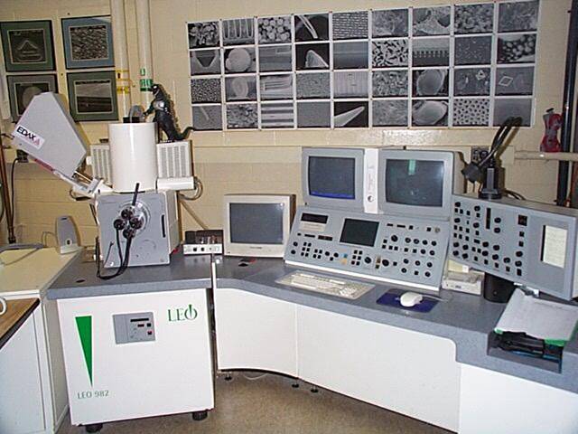
2. SEM observation
Several observation has been made on the following samples:
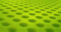
#1: Ag nano-rods/wire grown on a self-assembled InP porous substrate
#2: GaP crystal with self-assembled porous structures.
#3: Er particles/semi-continuous film grown on GaP porous substrate
#4 & #5: Gold nano-particle deposited on bulk GaAs substrate.
#6: Gold nano particles deposited on porous GaAs substructures.
All the samples are observed directly first with the SEM system for various magnifications. After that, Sample #1 and #3 are cleaved and the cross-sections are observed under the SEM, respectively.
3. X-ray analysis
To understand better the compositional structure of the artificial material, X-ray analysis is applied for samples #1, 4, 5 and 6 using the EDEX energy dispersive X-ray spectrometer. X-ray mapping is carried out for sample #4 for two major elements shown on the spectrum. Electron flight simulation is also applied to facilitate the interpretation of the X-ray spectrum.
4. Post-processing and Data Analysis
Particle size analysis is performed on one of the SEM photos of sample #4. In this way, the sizes of the nano-particles have been analyzed statistically. The distribution density and the average sizes of the particles on different samples are compared and related with the optical property of these samples.
Colorizing and other imaging processing technique are carried out in Photoshop and ImageJ to enhance the visual effect of the pictures.
|