| OPT 407 Course Project | Zhimin Shi, April 2006 |
 |
Microscopic Study on Artificial Metal-Semiconductor Nano-Materials |
|
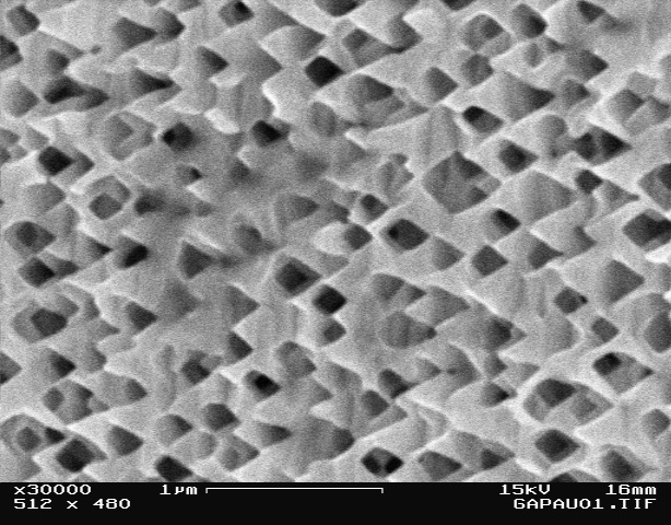
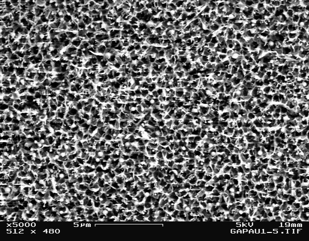
1. Surface topography There are three kinds of surface topography in our samples:
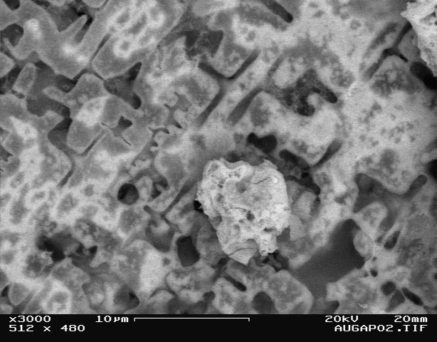
Fig. 4.1 Secondary Electron (SE)image of the surface of sample #2 (GaP) ii) Metal nano wires/rods grown on top of the Semiconductor porous structures. After the porous structures are formed, metal are deposited on the wall of the porous structures. From Fig 4.2, one can notice that the metal particles deposited on the surface has started to merge together into a semi-continous film. Note that the large particle in the center of the figure is a dust.
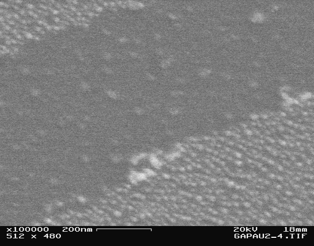
Fig. 4.2 SE image of the surface of sample #3 (Er on GaP) iii) deposited on to semiconductor on bulk semi-conductor surfaces. Whileobservaing such small features are very challenging, the imaging is successful with the help of adjust the focusing according to dust on the sample. The identification of these metal nano-particles on bulk GaAs surfaces are successful at a magnification of 100,000X. In the top plot of Fig. 4.3, a scratch is observed in the deposition area where the particle density of the gold is smaller. Sample #5 also has gold nano-particles on bulk GaP, but one immediately sees from the figure that the particle size is much larger, and the particle density is significantly smaller.
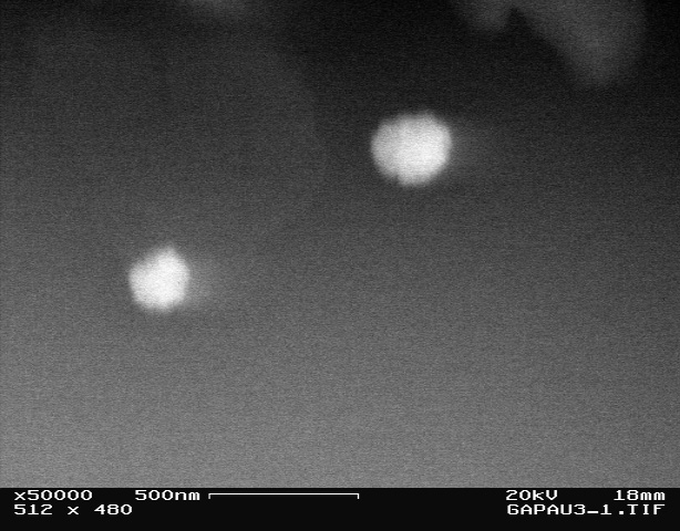
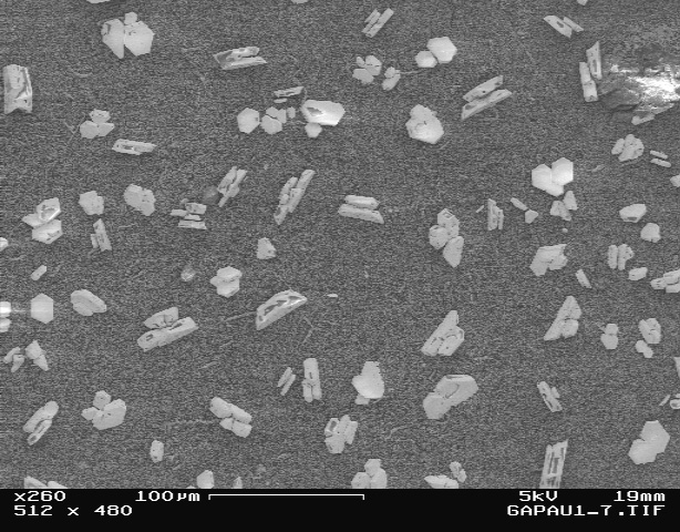
Fig 4.3 Top: SE image of sample #4 (Au on bulk GaP surface). A scratch is present in the region where the density of gold particles are much sparser. Bottom: SE image of sample #5 (Au on bulk GaP surface). The size of gold particle is larger, but the particle density is significantly smaller. iv) Metal nano-particles deposited on to semiconductor porous strucutres. The porous structures are very clear in Fig. 4.4, but it is hard to identify the gold nano-particles because the size of the particle is comparable or smaller than the porous structure of GaP. The large grains shown in the low-magnification image is not expected. Its components will be discussed later.
Fig. 4.4 Top: SE image for sample #6 (Au on GaP porous structures) with maginification of 260x;
|