| OPT 407 Course Project | Zhimin Shi, April 2006 |
 |
Microscopic Study on Artificial Metal-Semiconductor Nano-Materials |
|
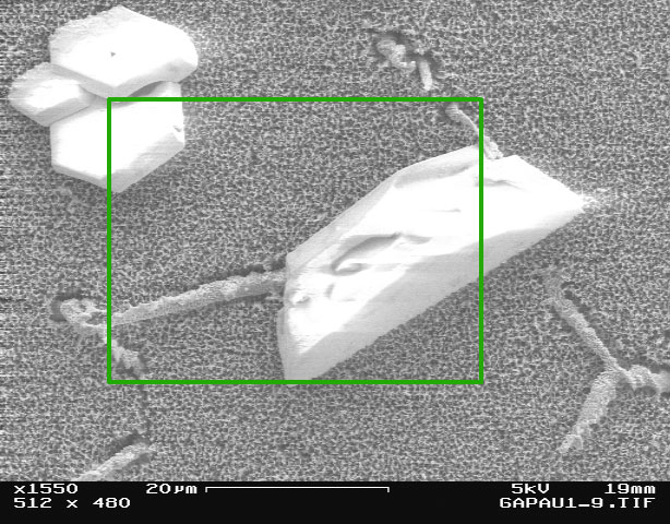
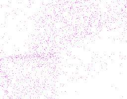
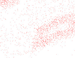
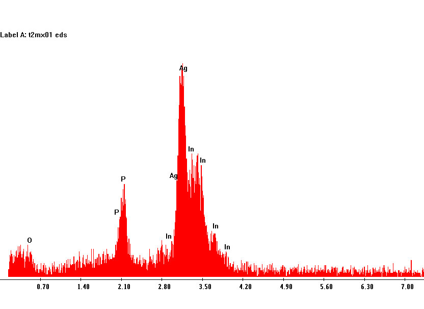
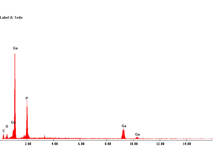
4. X-ray mapping X-ray mapping is performed for a region of Sample #6: Gold nano-particles on GaP porous structure. The L line of gallium and M line of gold are mapped. The mapping region (see Fig. 4.14) chosen is a section of porous structure with some suspicious large crystals fallen on the surface. As shown in Fig.4.15, it is clear to see that the gallium is uniformly distributed all over the region except those areas of large crystals. On the other hand, gold concentration is extremely high at the areas of large crystals, indicating that the crystals are gold, which is probably fallen on the surface during the deposition process. X-ray mapping is also carried out on samples #1 and #4, both of which has metal nano-particles deposited on semiconductor porous structures. However, the mapping does not show the exact position of metal nano-particles (for sample #4, there is even no X-ray signal from gold). The reason for this will be discussed in the analysis section. . Fig. 4.14 Approximate Region for X-ray mapping on sample #6. Fig. 4.15 X-ray mapping result for sample #6 (Au nano-particles on porous GaP) The left is mapping for Ga L line, and the right is mapping for Au M line.
|