| OPT 407 Course Project | Zhimin Shi, April 2006 |
 |
Microscopic Study on Artificial Metal-Semiconductor Nano-Materials |
|
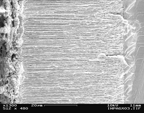
2.Cross-section structures The porous materials can be extended deep into the substrate. The maximum depth could be as large as a few hundred of microns (See Fig. 4.6). This offers possible future usages of such artificial materials without the support of thick substrate. As shown the SEM figures (see Fig. 4.5 and 4.6), the porous structure is well maintained at different depth position, with no change in porous size or collapse of pores. Furthermore, for samples with metal layers deposited on the wall, it can be seen that the metallic deposition is also quite uniform at different depth.
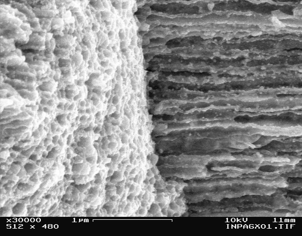
Fig. 4.5 The corner of top surface and cross-section for sample #1 (Ag on InP). The left part is the top surface with Ag deposited; the right part is the cleavage cross-section of the pores.
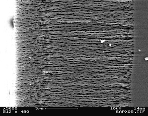
Fig. 4.6 The entire cross-section of sample #1 (Ag on InP). The most left part is the top surface with silver, the right most part is the substrate. The depth of the porous structure is measured to be around 66 um.
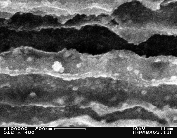
Fig. 4.7 A close look at the cross-section of the porous structure on Sample #1. The brighter dots clining on the wall of the pores are probably silver particles.
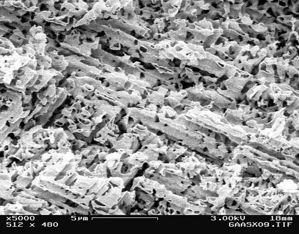
As one can see from Fig. 4.8, the cross-section is very different for samples #3, where Erbium is deposited on the surface of GaAs. One does not see very clear porous structures, but see multiple directions of the pores. This is because that the porous structure for GaAs is self-generated along the (1,1,1) direction. Since there are four possible (1,1,1) directions, the pores are penetrating into each other and therefore form complicated structures. Meanwhile, one do not see the Er particles, which is because Er has formed new compound material with the GaAs.
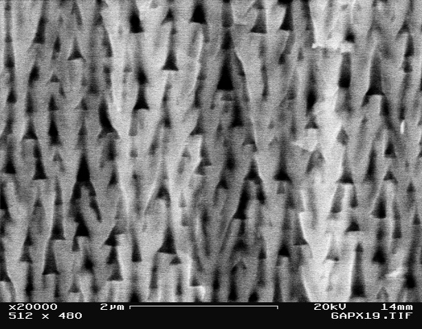
Fig 4.8 Cross-section SE image on sample #3 (Er on GaAs). The porous structure for GaP (see Fig. 4.9) is similar to the case of InP, in which the pores are grown perpendicular to the surface. However, one notice that the wall of the GaP pores is not as smooth as that of the InP. Instead, it exhibit some saw-tooth like edge as shown in Fig. 4.10. This difference is partly due to the material difference, and partly due to the etching conditions.
Fig. 4.9 The entire cross-section of sample #2 (GaP). The most left part is the top surface, the right most part is the substrate. The depth of the porous structure is measured to be around 15 um.
Fig. 4.10 A close look at the cross-section of the porous structure of sample #2 (GaP).
|