| OPT 407 Course Project | Zhimin Shi, April 2006 |
 |
Microscopic Study on Artificial Metal-Semiconductor Nano-Materials |
|
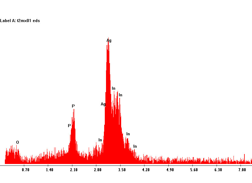
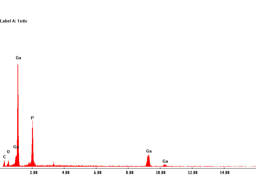
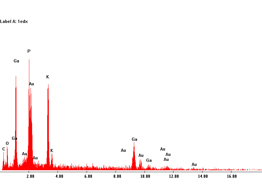
3. X-ray spectrum Besides secondary electrons and backscattered electrons, a third most useful signal produced by the interaction of the electron beam with the specimen in a SEM is the x-ray, since the energy of the X-ray is equal to the energy difference between the two electron orbitals, and therefore can be used to determine the material composition of the sample. The present SEM system has a energy dispersive spectrometer to analyze the X-ray signals. X-ray spectrum is taken for samples #1, #4 and #6 with accelerating voltage of 20kV. The spectrums are shown in Figs. 4.11-4.13, respectively, and the result is quite as expected since the samples are fabricated purposely. It should be noted that the expected gold peaks are missing in the spectrum of sample #4. which is against normal expectation. This abnormality is probably because the size (and the volume) of the gold nano-particles is too small that there are hardly any X-ray generated from the interaction between gold and electrons. This issue will be studied further later in the analysis section.
Fig. 4.11 X-ray spectrum from sample #1 (Ag on porous InP)
Fig. 4.12 X-ray spectrum from sample #4 (Au nano-particles on bulk InP)
Fig. 4.13 X-ray spectrum from sample #6 (Au nano-particles on porous InP)
|