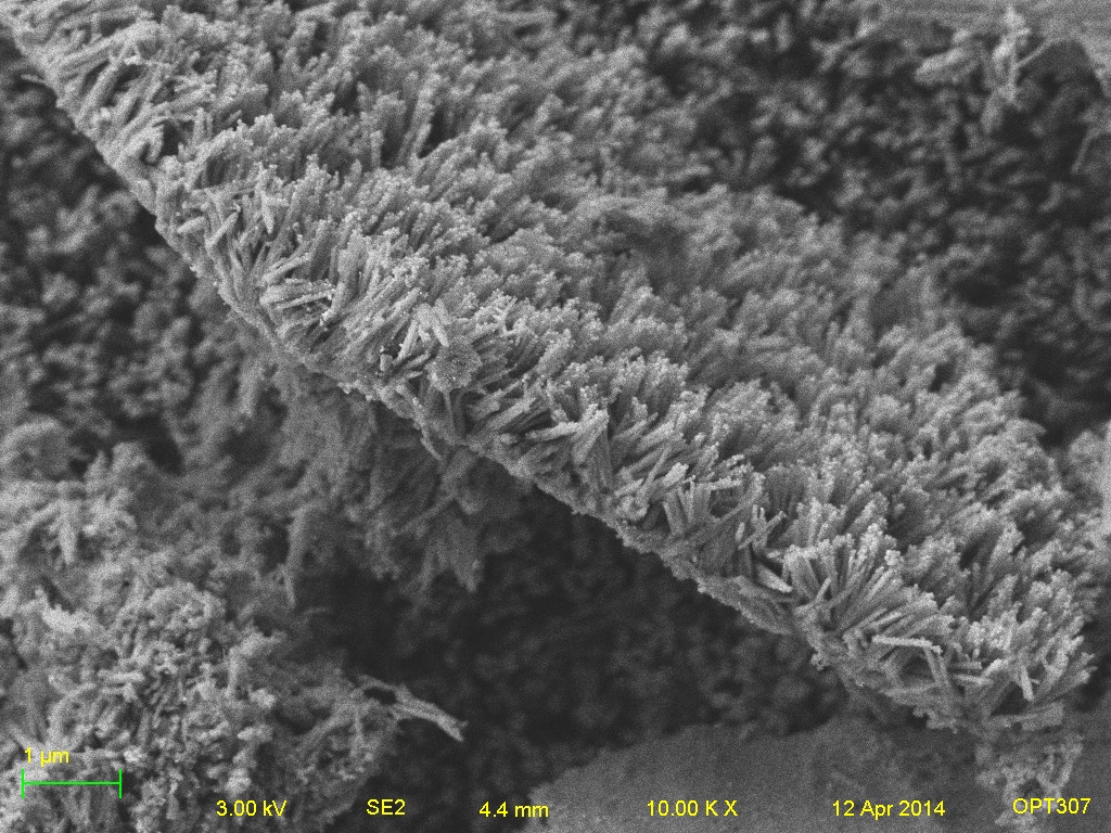
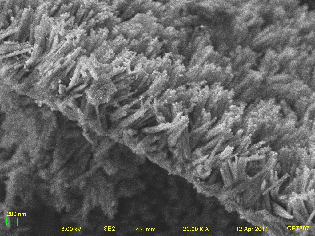
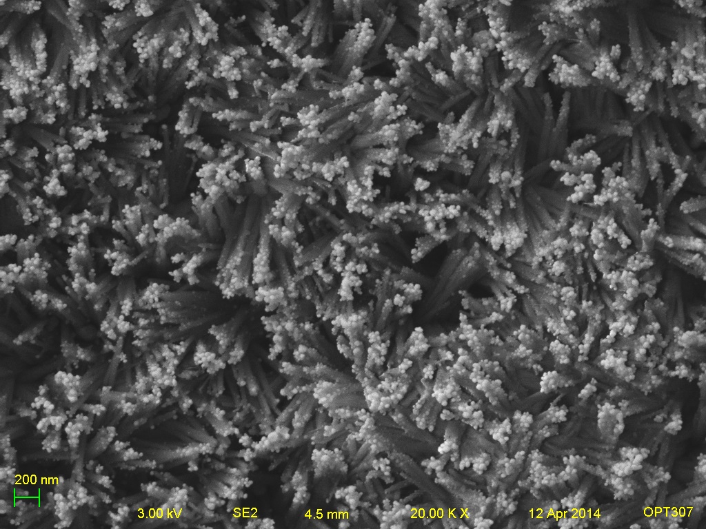
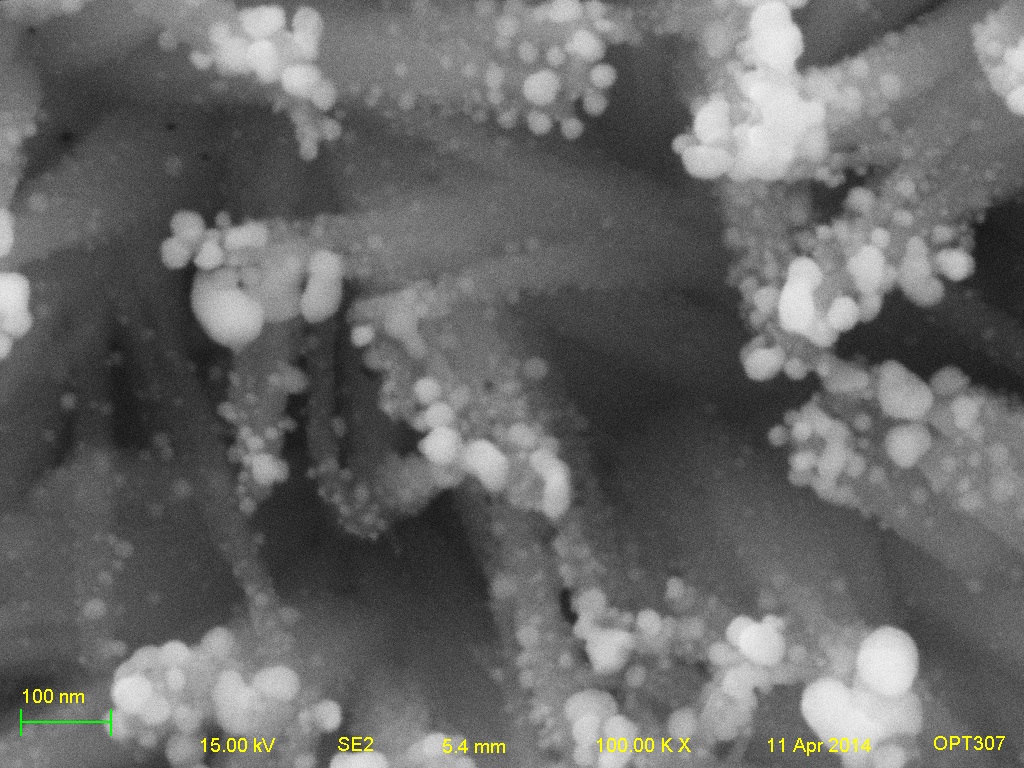
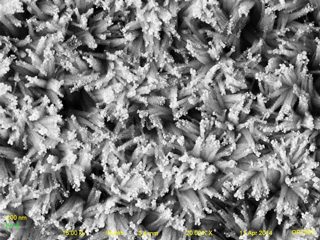
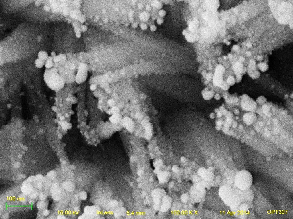
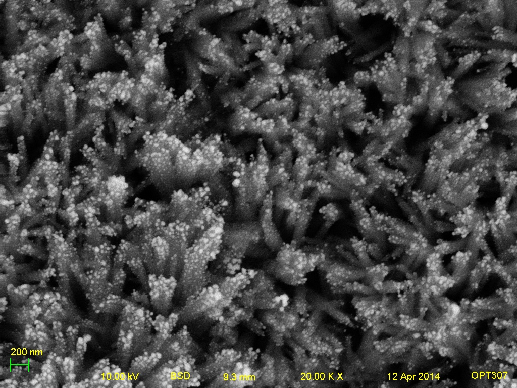
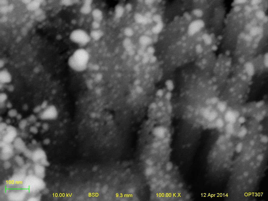
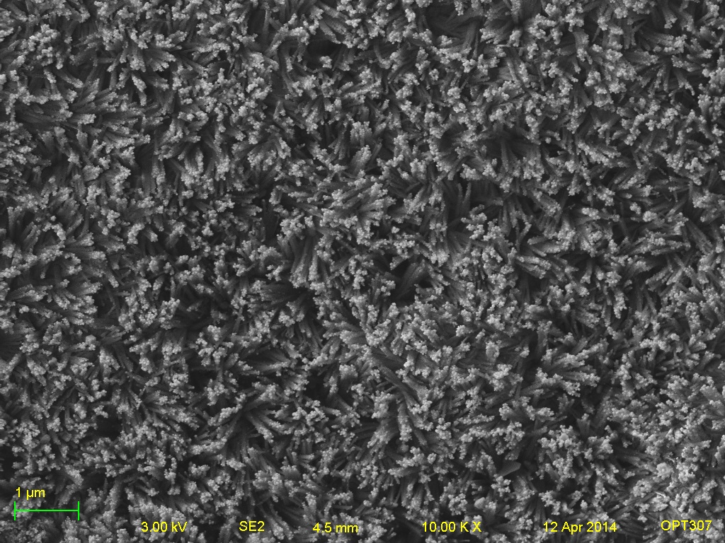
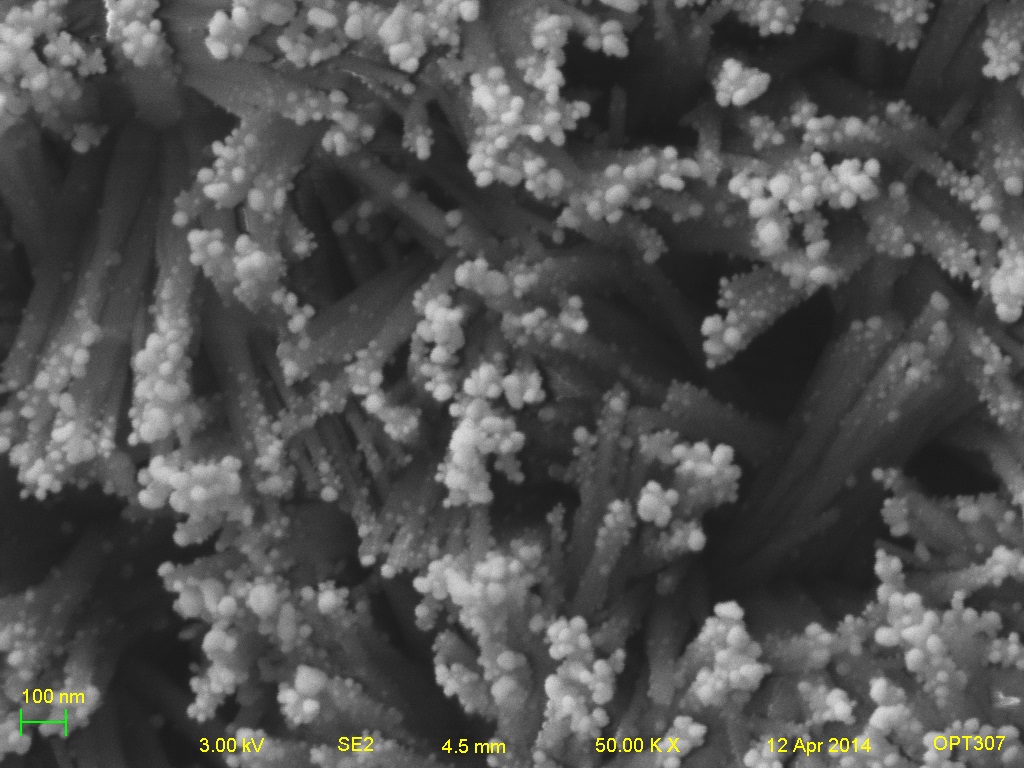
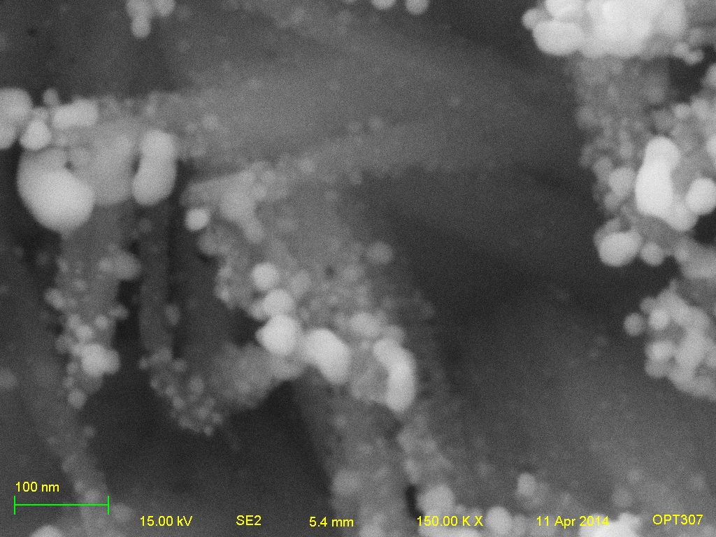
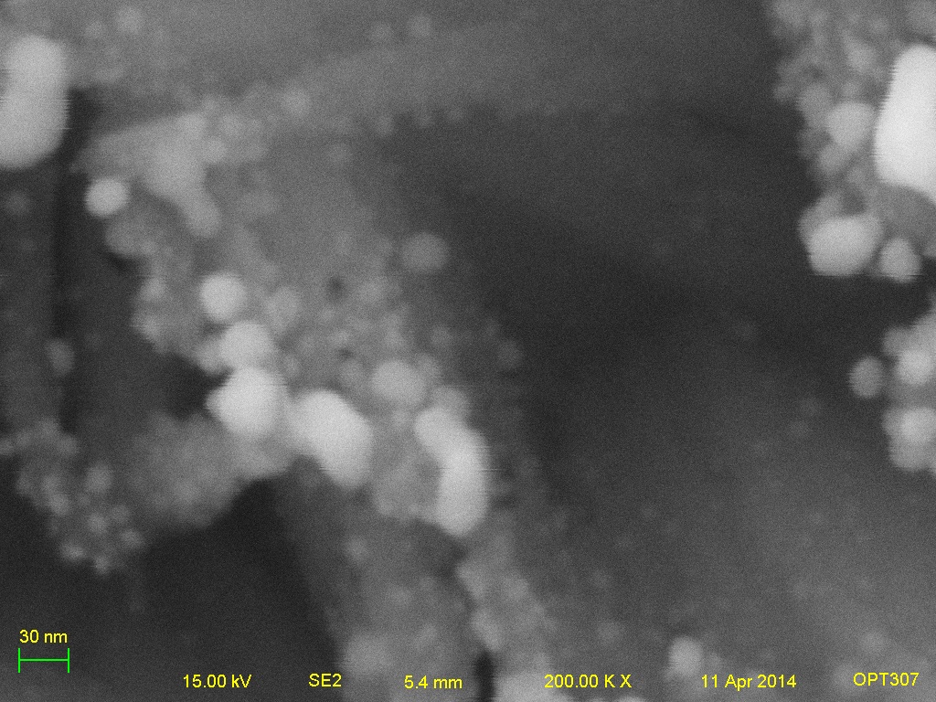
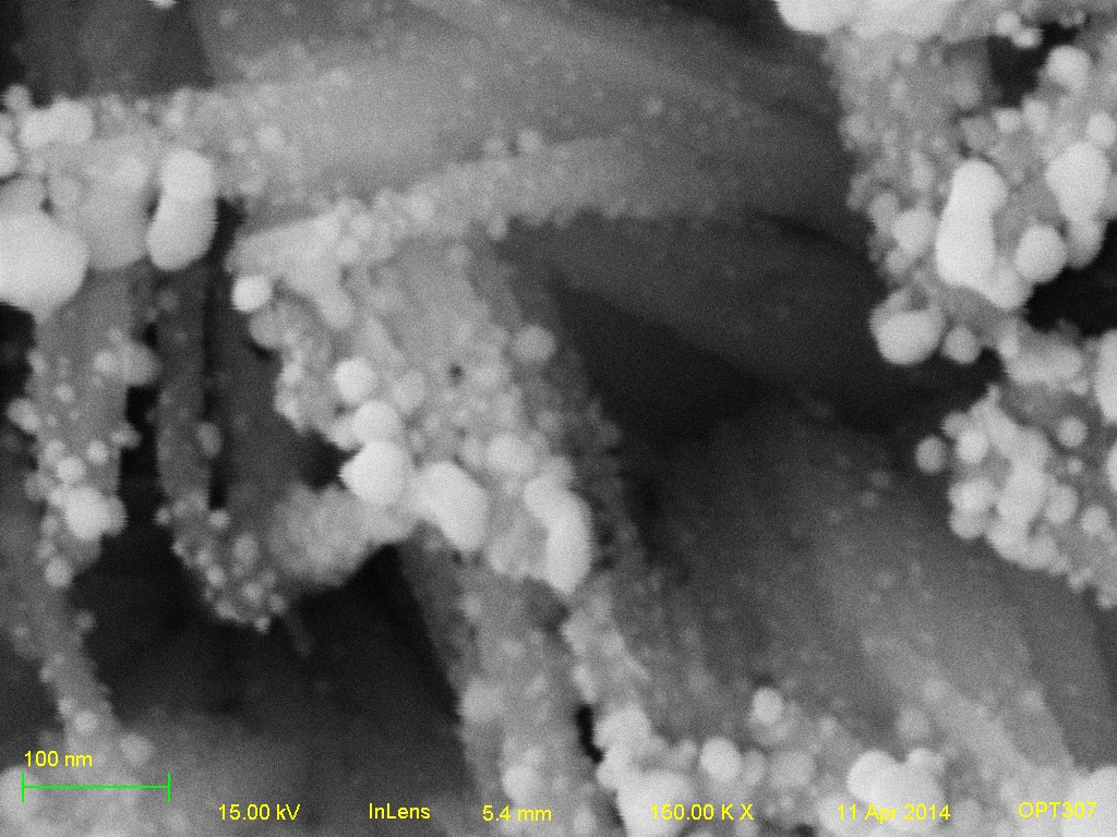
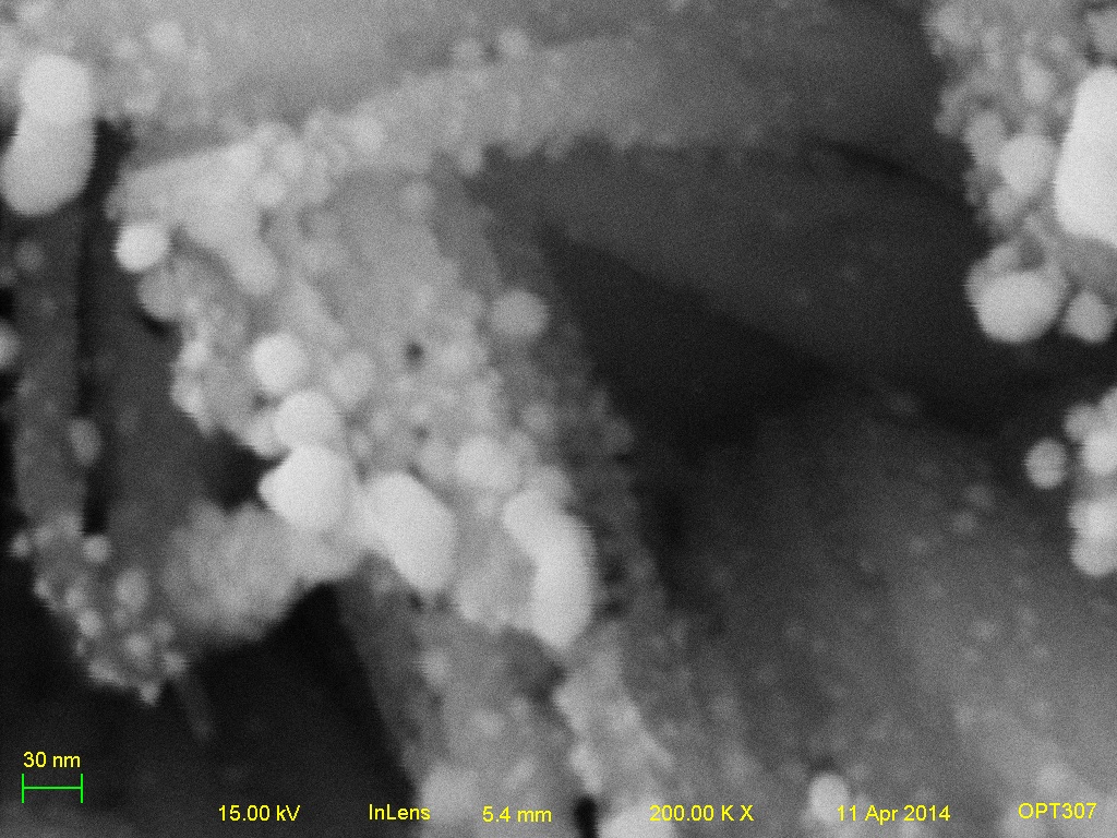
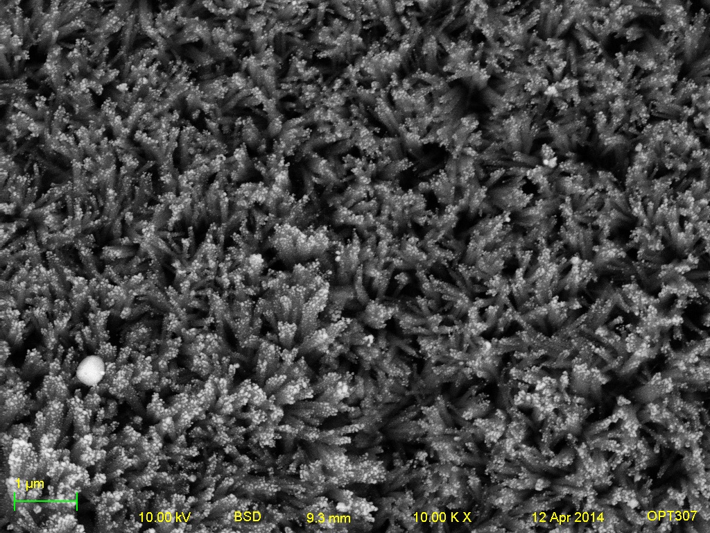
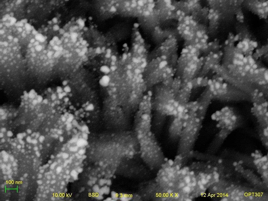
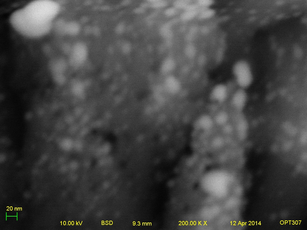
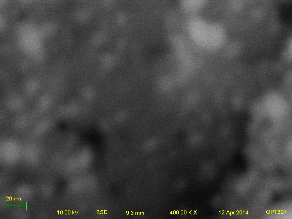
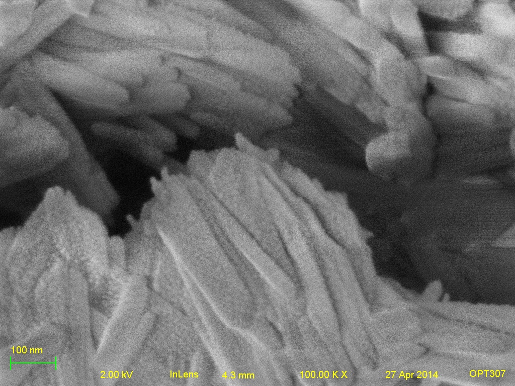
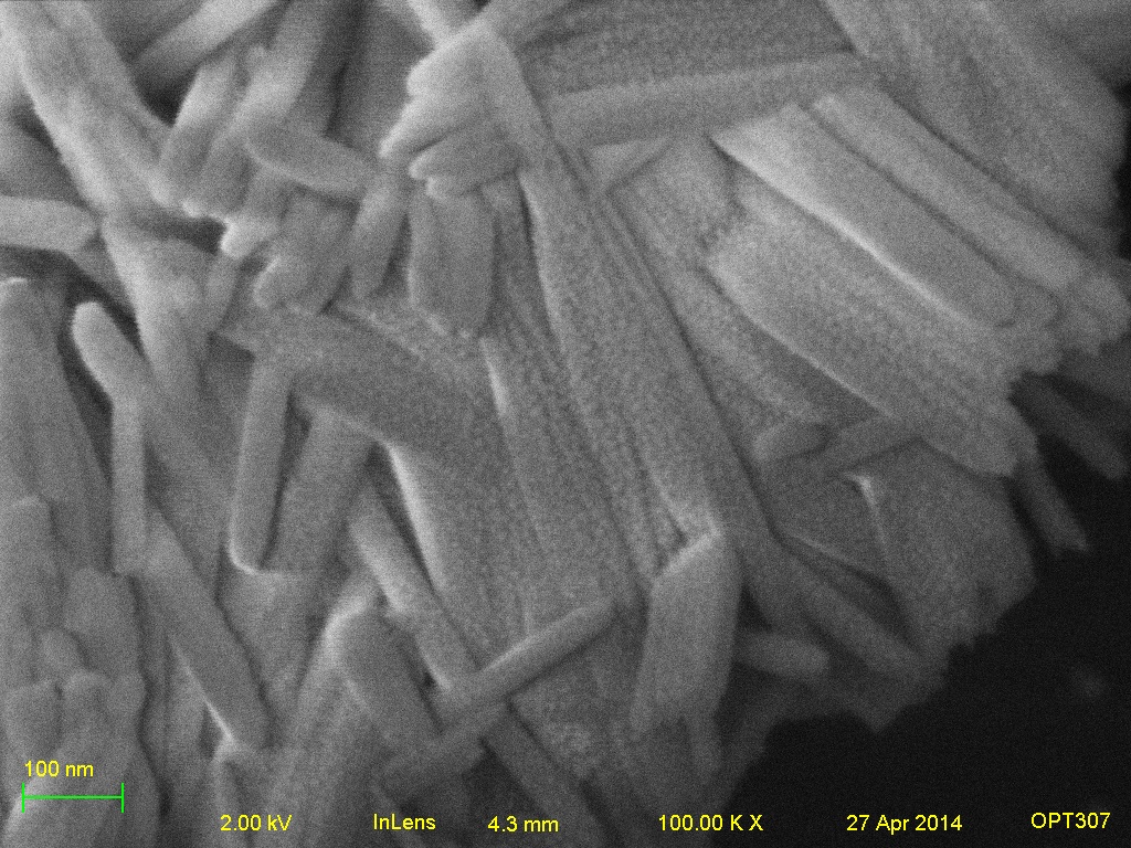
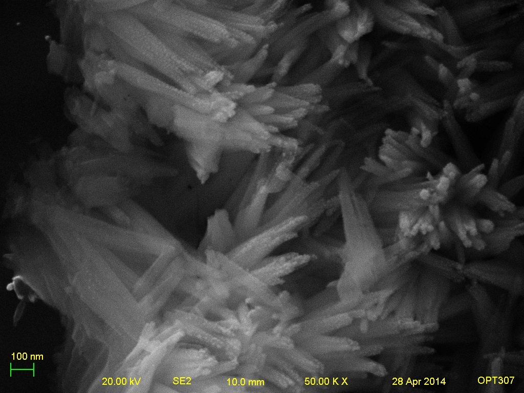
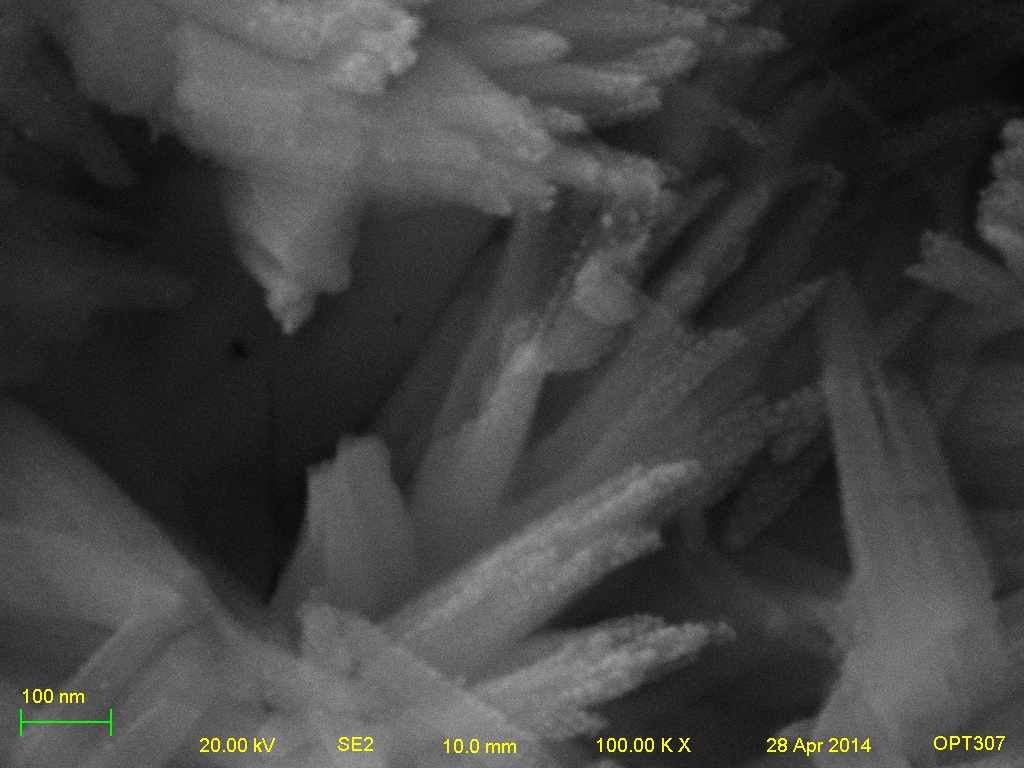
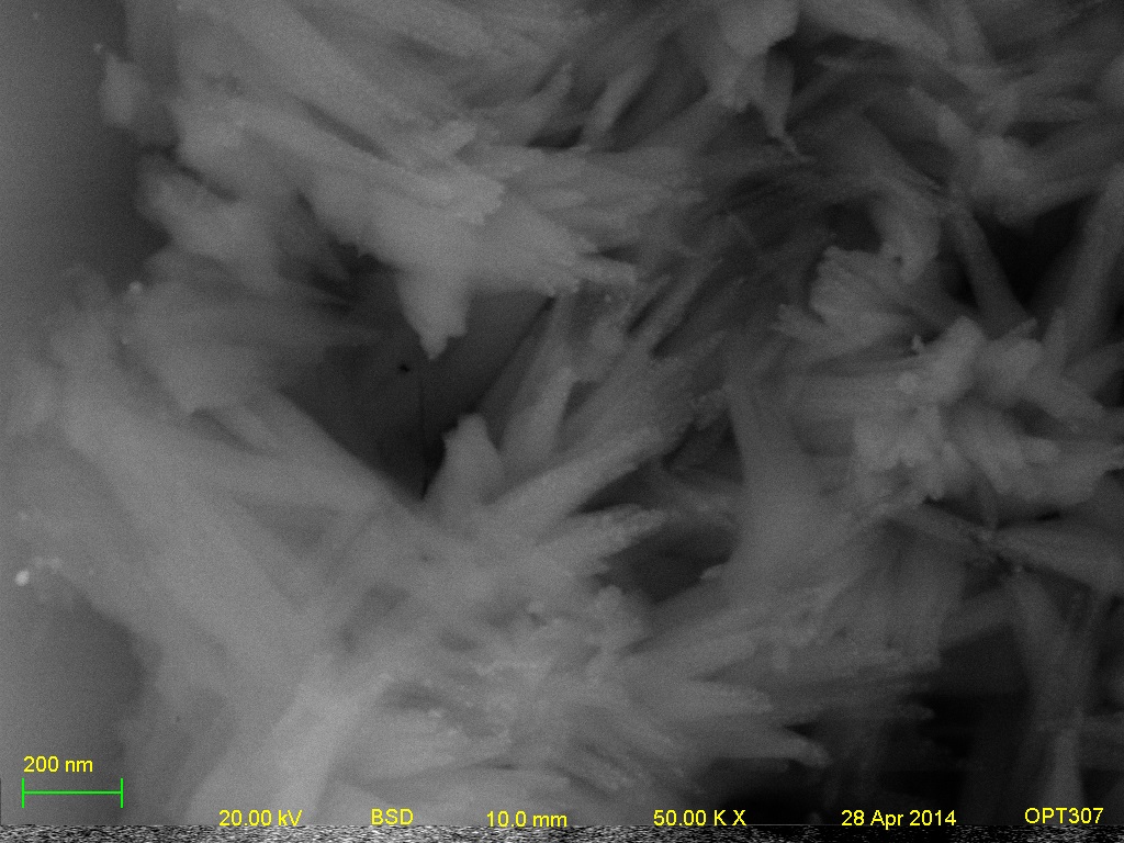
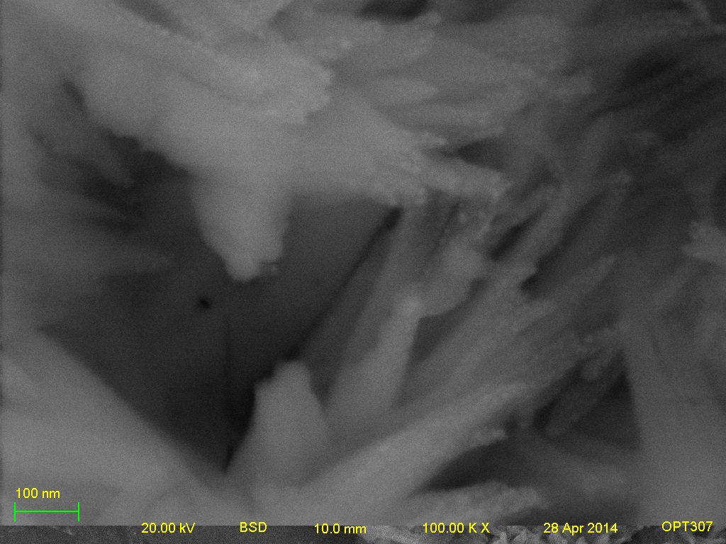
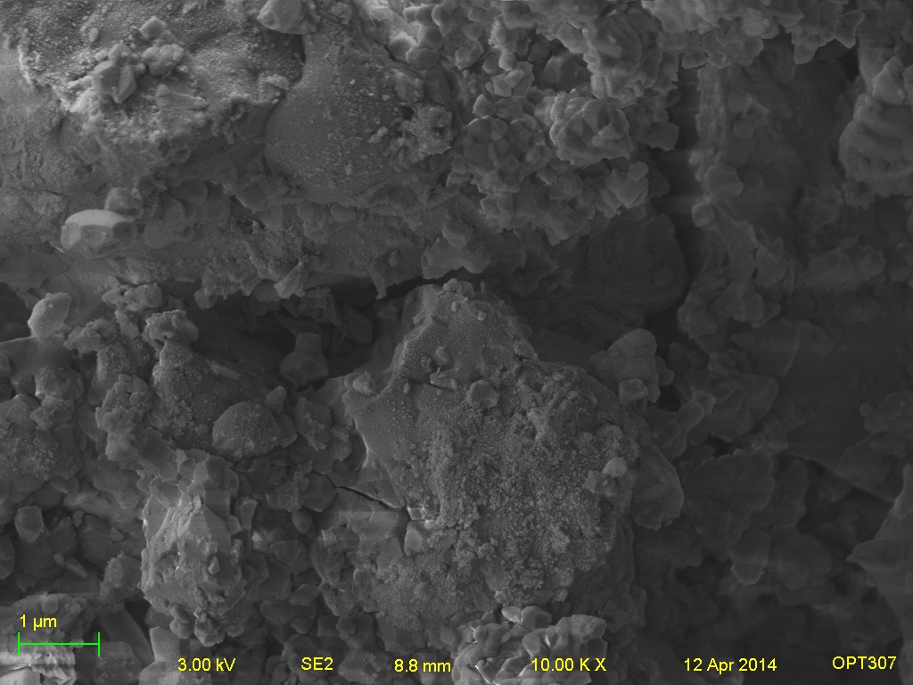
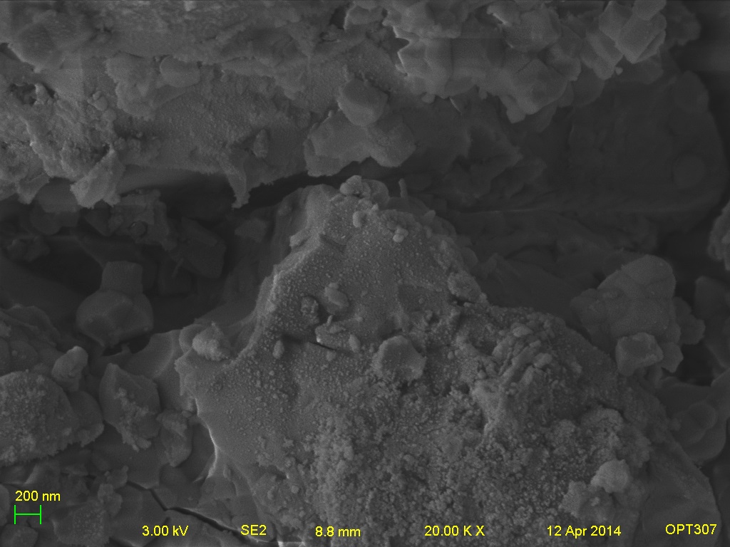
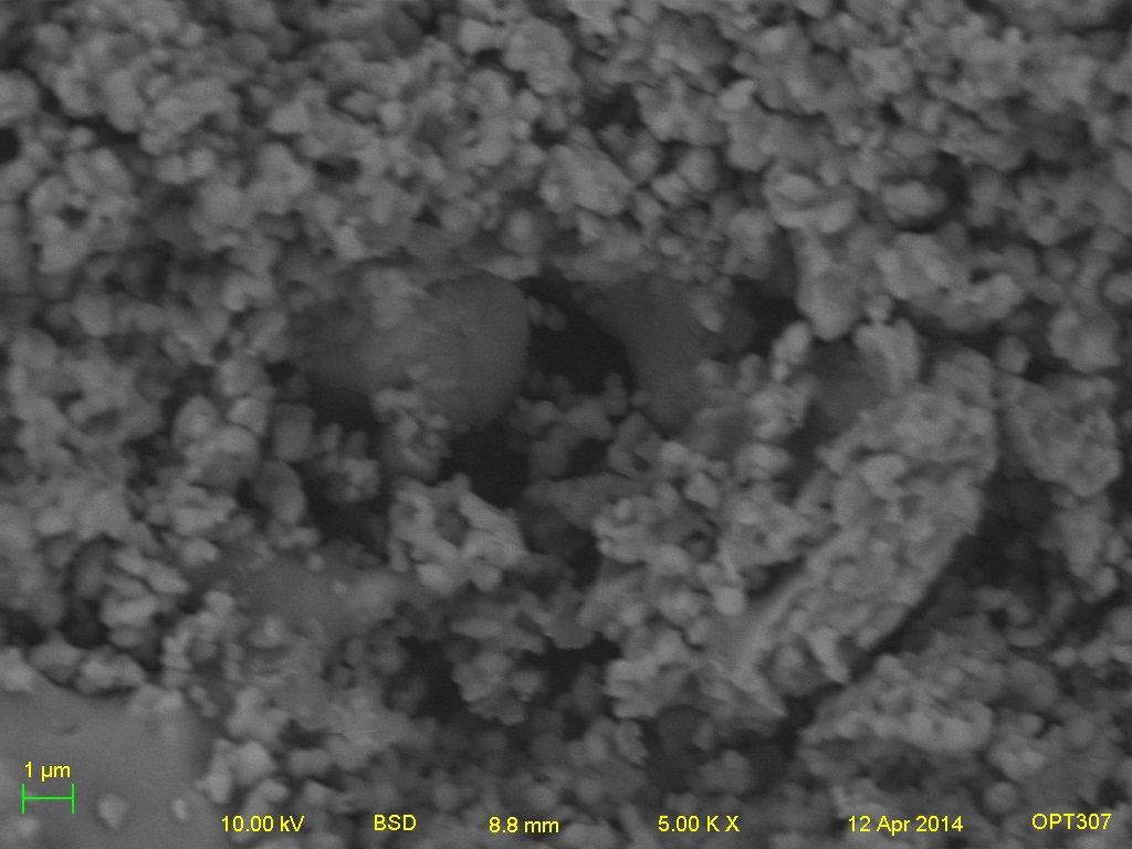
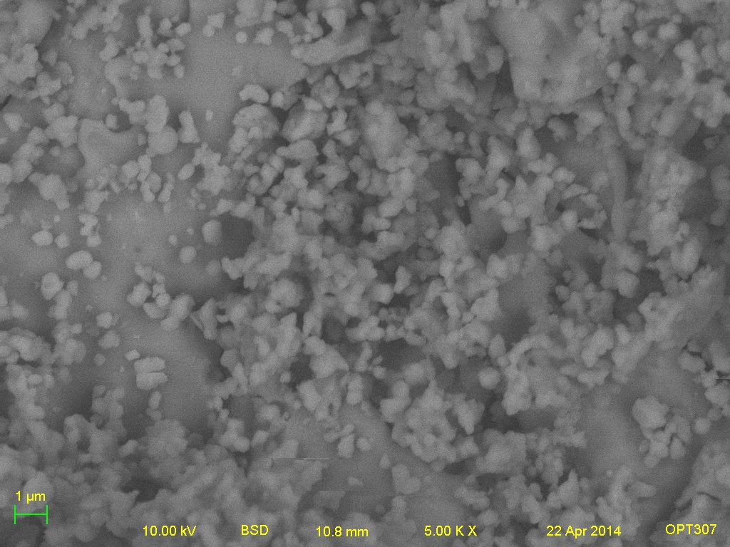
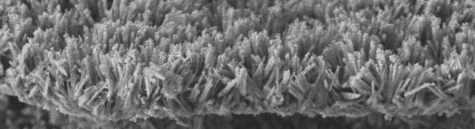
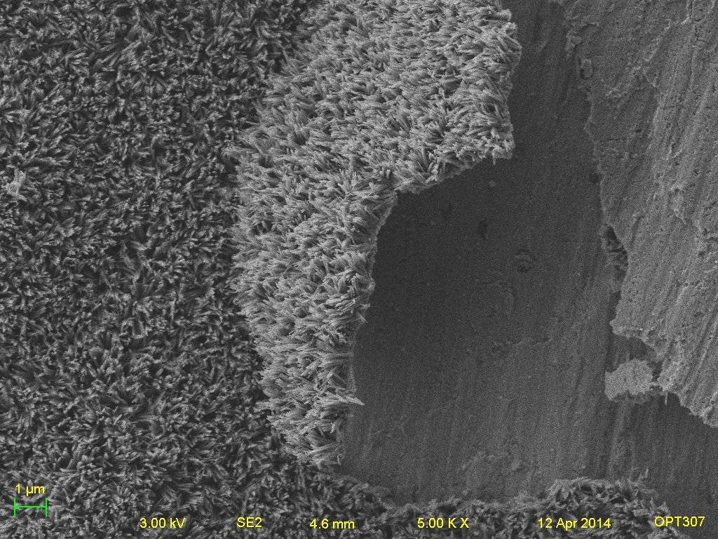
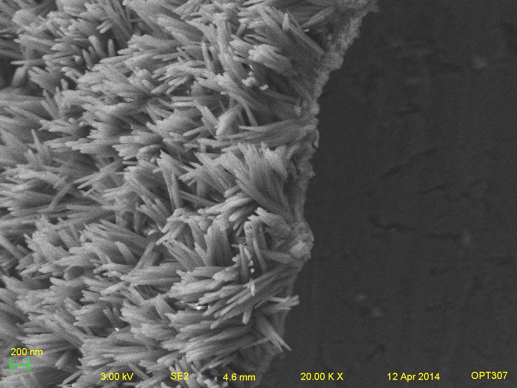
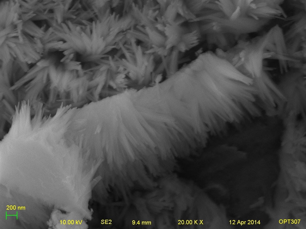
Electrochemically Deposited Hydroxyapatite (HAP) Coating

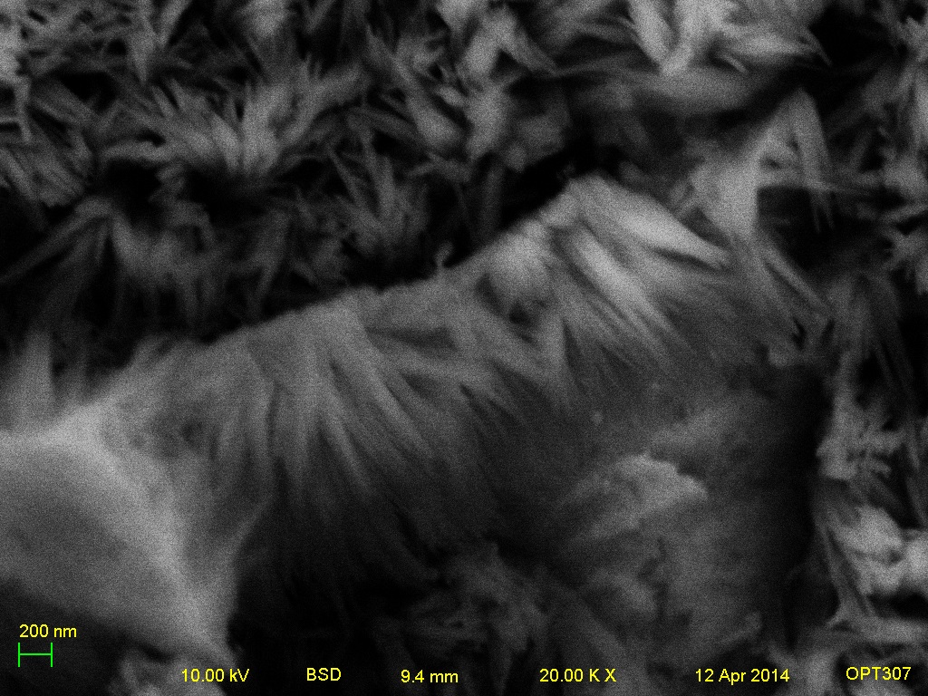
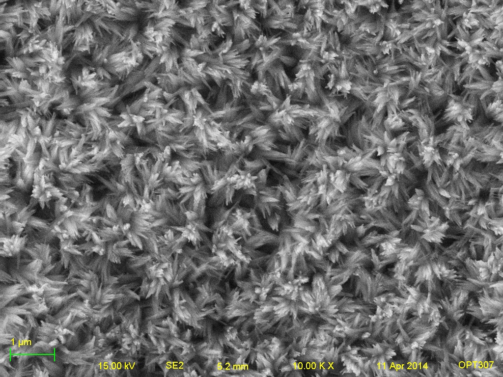
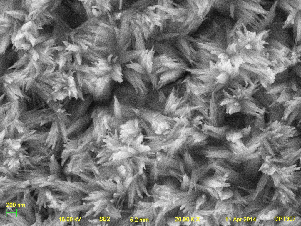
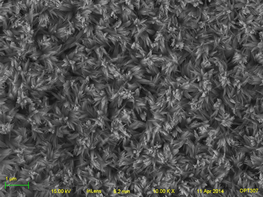
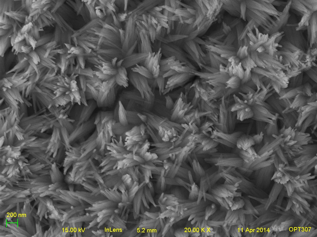
The following images depict the crystal morphology and coating layer of the electrochemically deposited HAP before any addition of silver nanoparticles.

The side views were imaged by macroscopically scratching the sample coating with a razor blade and imaging a slightly dislodged portion of coating.

HAP Side View (SE2) (1) 5kx (2) 20kx
HAP Side View Imaging Mode Comparison (1) SE2 (2) BSD


The top views were imaged using secondary electron signals, both SE2 and InLens, and a backscattered electron signal (BSD). For comparison purposes the sample was imaged at magnifications of 10kx and 20kx for each imaging technique.

HAP Top View (SE2) (1) 10kx (2) 20kx
HAP Top View (InLens) (1) 10kx (2) 20kx
HAP Top View (BSD) (1) 10kx (2) 20kx

Electrochemically Deposited Silver Nanoparticles on HAP

The following images are representative of the size, placement, and relative pervasiveness of the silver nanoparticles resultant from the electrochemical deposition process.

Deposited Ag Side View (SE2) (1) 10kx (2) 20kx


Similar to the HAP samples, the top views of the deposited silver samples were imaged using both secondary electron signals, SE2 and InLens, and a backscattered electron signal (BSD). For comparison purposes the sample was imaged at magnifications of 20kx and 100kx for each imaging technique to highlight the size and placement of the nanoparticles.

Deposited Ag Top View (SE2) (1) 20kx (2) 100kx
Deposited Ag Top View (InLens) (1) 20kx (2) 100kx
Deposited Ag Top View (BSD) (1) 20kx (2) 100kx


The sample was imaged at many other magnification settings for each imaging technique. While 20kx and 100kx were representative and chosen for comparison, all the micrographs collected are listed below for reference.

Deposited Ag Magnification Comparison (SE2) (1) 10kx (2) 20kx (3) 50kx (4) 100kx (5) 150kx (6) 200kx
Deposited Ag Magnification Comparison (InLens) (1) 20kx (2) 100kx (3) 150kx (4) 200kx
Deposited Ag Magnification Comparison (BSD) (1) 10kx (2) 20kx (3) 50kx (4) 100kx (5) 200kx (6) 400kx

Sputtered Silver Nanoparticles on HAP

The following images are representative of the size, placement, and relative pervasiveness of the silver nanoparticles resultant from the sputtering process displayed through all three types of electron signals. These images were done at the higher magnifications of 50kx and 100kx given the tiny size of the nanoparticles. Fewer images are available of this method for creating silver nanoparticles than the deposited Ag due to the difficulty of obtaining decent micrographs; this sample is less conductive and sputtercoating a conductive layer onto the sputtered nanoparticles would destroy the integrity of the sample's surface qualities.

Sputtered Ag (InLens) (both 100kx)
Sputtered Ag (SE2) (1) 50kx (2)100kx
Sputtered Ag (BSD) (1) 50kx (2)100kx

Plasma Sprayed Hydroxyapatite Coating

For the purpose of comparing the novel, electrochemical deposition of hydroxyapatite and its resulting crystal morphology to current industry standards for hydroxyapatite coatings, a sample of plasma sprayed HAP on a titanium substrate was obtained and cursorily imaged. See the following figures.

Plasma Sprayed HAP (SE2) (1) 10kx (2) 20kx
Plasma Sprayed HAP (BSD) (both 5kx)