X-Ray Microanalysis

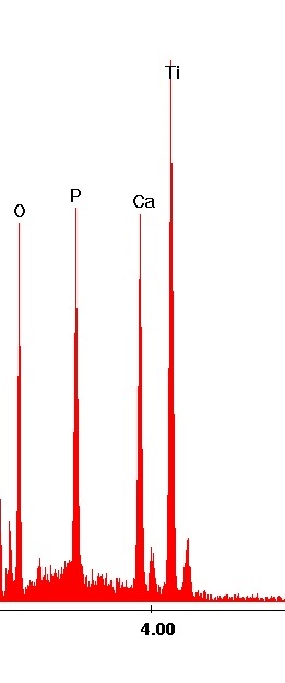
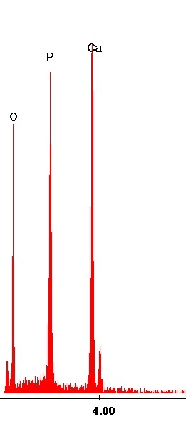
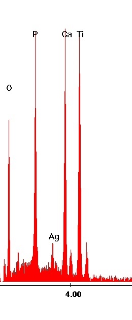
Energy Dispersive Spectra (EDS) were used to analyze the elemental composition of each of the four types of samples. Peaks were identified within the EDAX software and were verified based on knowledge of hydroxyapatite (calcium phosphate crystal) and the deposition process (includes use of sodium chloride and silver nitrate). Occassionally, the EDS would register Na and/or Cl within the sample; this was deemed to be residue on the surface of the crystals from the salt in the deposition solution and was ignored if present.

Representative Spectra and Peak ID (Energy in kV vs Relative Abundance) (1) HAP (2) Plasma Sprayed HAP (3) Deposited Ag (4) Sputtered Ag


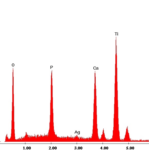
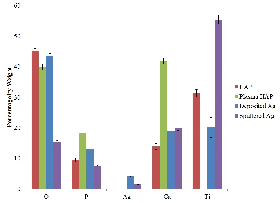
The spectra indicate that indeed all the coatings include O, P, and Ca, the main elements in hydroxyapatite. The presence of a Ti peak in all but the plasma sprayed HAP sample suggests that the electrochemically deposited HAP coating is so thin that the beam's interaction volume includes some aspect of the titanium substrate beneath, whereas the plasma sprayed HAP coating is much thicker. Finally, the presence of a Ag peak is anticipated and observed on the two samples where an attempt was made to add silver to the coating. In addition, using the EDAX software, the relative abundance (percentage by weight and percentage by atomic amount) of each element within each sample was calculated and the average values of those categories are shown below.

Relative Abundance of Elements (1) Weight % (2) Atomic %


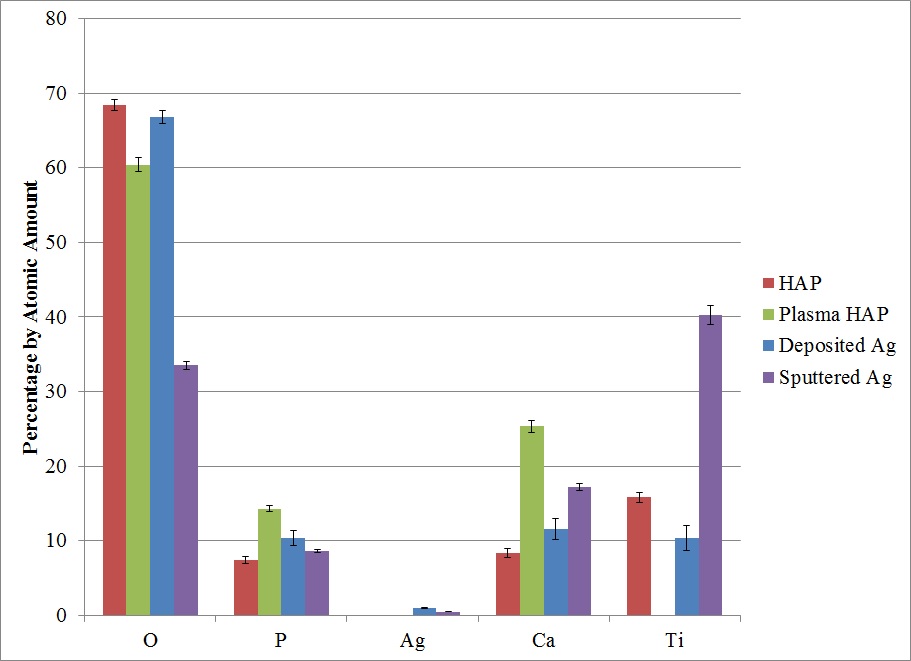
The above data indicates that EDS observes a much higher abundance of silver, particularly in relation to the abundance of P and Ca from the HAP, in the electrochemically deposited silver samples as opposed to the sputtered silver samples.

Relative Silver Abundance
  Ag:O (Wt%) Ag:P (Wt %) Ag:Ca (Wt %)
Deposited Ag 0.095 0.32 0.22
Sputtered Ag 0.099 0.20 0.077


Using the relative atomic abundances of the elements, in particular, P and Ca, the exact chemical make-up of the crystal structure can be explored. Hydroxyapatite should have three Ca atoms for every 5 P atoms, but it has been know to vary widely from this ideal when in crystal structures such as this HAP coating. Not surprisingly, plasma sprayed HAP is much closer to this ideal, whereas the HAP created from electrochemical deposition is Ca deficient due to the process. One should expect HAP, Depositied Ag, and Sputtered Ag to be identical since the Ca and P all come from the same HAP structure, however, surprisingly, the sputtered Ag samples deviate radically. This points to the large amount of error and variability which exists in X-ray microanalysis of rough samples like these with large amounts of free space (very non-ideal, non-homogenous calculation conditions).

Relative Ca:P Ratios
  Ca:P (At %)
Ideal HAP 1.67
HAP 1.13
Plasma HAP 1.78
Deposited Ag 1.12
Sputtered Ag 2.00


Atomic Force Microscopy

The electrochemically deposited silver nanoparticle sample was imaged on the Atomic Force Microscope (AFM) in an attempt to gather topographical information and images, and also to measure the roughness of the coating as a whole and that of the silver nanoparticles on the individual crystals.

AFM Micrographs of 30 um x 30 um section of Deposited Ag on HAP (1) 2D (2) 3D
AFM Micrographs of 6 um x 6 um section of Deposited Ag on HAP (1) 2D (2) 3D
AFM Micrographs of 1.0 um x 1.0 um section of Deposited Ag on HAP (1) 2D (2) 3D


With the simple, preliminary AFM analysis of this sample a further, albeit somewhat limited, understanding of the HAP crystals and the nanoparticles is gained. More extensive AFM work must be done to verify these results. However, the first set of images suggest that there is obviously variation in crystal heights, but even within a larger context, there are over 1 um variations in topography between areas of crystal growth. The second set of AFM data begins to allude to the shape of the individual HAP crystals, indicating that perhaps each crystal has a very-defined triangular cross-section. Finally, the third set of images narrows onto one of these triangular regions, presumably, the surface of a HAP crystal. The variations in topography along its surface are minimal, less than a few hundred nm, and thought to be caused by the silver nanoparticles at the tip of the crystal.

Using the AFM's software, an 'Average Roughness' was calculated from each of the above three micrographs. Granted, given the complexity and non-uniformity of the crystal layer, the drastic height variations, and the abundance of sharp edges, AFM is not an excessively reliable technique in these circumstances. Regardless, the cursory evaluation of roughness offers insight into the crystal and nanoparticle sizes and variations. The roughness was calculated over the entire area imaged, with the exception of the final roughness which is only over the relatively "flat" area of the image, the crystal surface and not edge.

Average Roughness
  Average Roughness (nm) Root Mean Square Roughness (nm)
30 um x 30 um (HAP coating) 221 274
6 um x 6 um (crystal tops) 86.8 108
0.5 um x 0.5 um (nanoparticles) 26.5 31.3

ImageJ Analysis

Several of the recorded micrographs were analyzed using the ImageJ software, allowing for characterization of various aspects of the images and samples. First, coating thickness was assessed using the images of various side views. Several measurements were taken on each micrograph and averaged together over many diferent side view images. It was found that the average HAP coating thickness was 1030 ± 50 nm; essentially, the electrochemical deposition of hydroxyapatite produces a crystal layer of about 1 um thick.

Coating Thickness Measurement Procedure