|
|
X-ray X-ray characterization
was done using the STEM HAADF EDX in the TEM and EDAX in the
SEM. X-ray characterization in the
center of the spheres produced different results compared to
the outer radius of the sphere, which is due to the fact that
the spheres are somewhat hollow. The
SEM spectra showed very large peaks for Al and for the 20kV
spectra it was very difficult to find the Ag and Pd peaks.
With accelerating voltages of 20kV and 10kV the interaction
volume was mostly in the aluminum sample stub since the nanoparticles
are so small, which is why the Al peaks were so large.
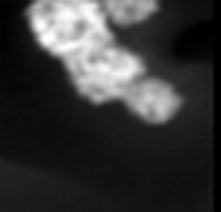
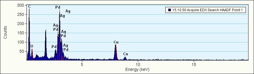 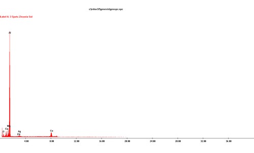 Figure 13:Low concentration Ag-Pd NPs spectra from TEM and SEM, respectively 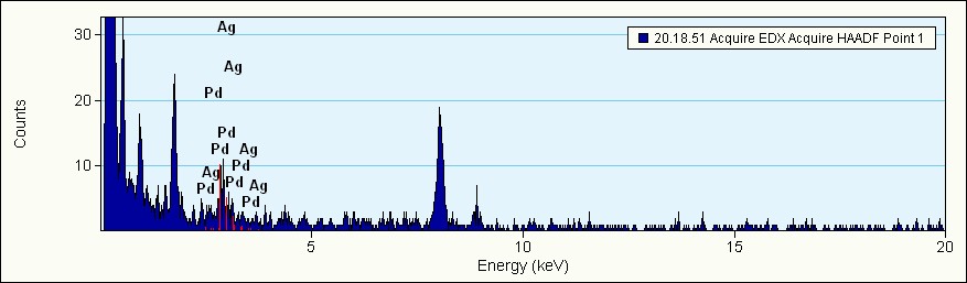 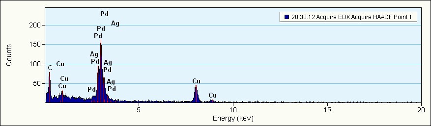   Figure 14: Medium concentration Ag-Pd NPs spectra for the center and outer radius of the sphere in the TEM and 10kV and 20kV accelerating voltages in the SEM 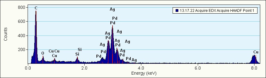 Figure 15: HIgh concentration Ag-Pd NPs spectra Elemental Mapping Elemental mapping
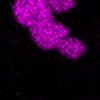
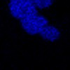
confirmed that Ag and Pd are both present in the nanoparticles. Both Ag and Pd are uniformly distributed across the nanoparticles.
Line scans across the particles reveal that there is
less Ag and Pd in the center of the spheres, which confirms
that the spheres are hollow, or at least somewhat hollow.
 Figure
16: Low concentration Ag-Pd NPs STEM image and elemental mapping
for Ag-L and Pd-L, respectively
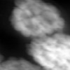 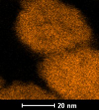
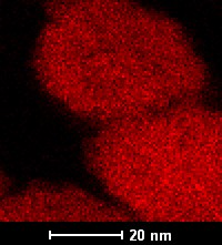 Figure 17: Medium concentration Ag-Pd NPs STEM image and elemental mapping for Ag-L and Pd-L, respectively 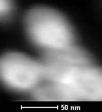 
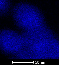 Figure 18: High concentration Ag-Pd NPs STEM image and elemental mapping for Ag-L and Pd-L, respectively 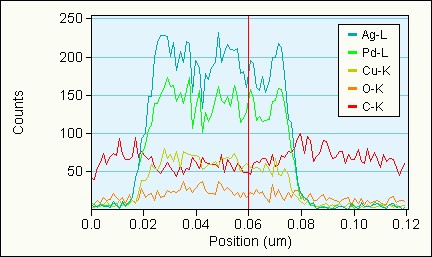 Figure 19:Low concentration Ag-Pd NPs line scan across center of nanoparticle with all elements present 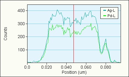 Figure 20: Medium concentration Ag-Pd NPs line scan with just Ag-L and Pd-L present 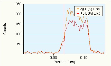 Figure 21: High concentration Ag-Pd NPs line scan with just Ag-L and Pd-L present |