
2007 News Archive
Adjustable Ultrathin Nano-Filter Separates Biological Molecules
Researchers at the University of Rochester have created an ultrathin porous nanocrystalline silicon membrane that filters biological molecules. The new filter, reported in the February 15, 2007 issue of Nature, is so thin and efficient that it enables scientists to separate and retain "collections" of two sizes of molecules. The pores can be adjusted to separate molecules of most any size, to separate similarly sized molecules carrying different charges, and to transport small molecules through the membrane much faster than current methods. Possible applications of the nano-filters include renal dialysis, whereby a device can remove toxins that failing kidneys no longer cleanse from the blood; precision air filters; membrane-based chromatography systems; and microfluidic systems requiring highly efficient separations.
The present way of separating biological molecules is to use a sponge-like filter that is 1,000 times thicker than the new nano-membranes. Although smaller molecules can enter and pass through thick filters, many remain within the matrix, clogging pores and eventually rendering the filter useless. This also leads to significant sample loss, so labs can only capture and retain the larger molecules that fail to enter the filter.
The transport rate, whether it's diffusive transport or forced flow transport, scales inversely with thickness. The thinner the membrane, the less resistance there is to molecules flowing through it, and also, the faster things diffuse across it.
The ultrathin nano-membrane ranges from three to twenty-five nanometers thick. Its nano-pores can be less than five nanometers or as much as fifty nanometers in diameter. Team member Christopher C. Striemer (Research Associate, Electrical & Computer Engineering) notes, "Despite the nanoscale thickness and porosity, the membrane material remains stable under various temperatures and pressures. The three-nanometer-thick membranes are not very stable. Seven-nanometer membranes are more robust, and our standard fifteen-nanometer-thick membranes are very strong, supporting an atmosphere of differential pressure for macroscopic sizes."
Basically, the researchers form the membranes and pores on silicon wafers using standard procedures. As Distinguished Professor Philippe M. Fauchet (Electrical & Computer Engineering) says, "You can put a silicon facility together, and you can start mass producing these nano-membranes very easily."
Another member of the team, Assistant Professor James L. McGrath (Biomedical Engineering), adds that "silicon is a very strong material, and it can withstand temperatures far higher than all the other organic-based materials currently are used for membranes. And also, for a given thickness, these new nano-membranes are far stronger than any polymeric material that currently exists."
"In addition," says Thomas R. Gaborski (PhD Candidate, Biomedical Engineering), "one of the most exciting aspects of our discovery is that, by changing the parameters we use while creating the membranes, we're able to customize the pore sizes -- that is, the actual filters -- in the membranes. So if we change process temperature slightly, to name one example, we get filters with slightly different pore sizes."
Left Image (Below)--An artist's rendering of how the nano-membrane separates small and large molecules. The small (red) molecules pass through the pores. Notice that all of the larger (yellow) molecules remain on top of the nano-membrane and do not get stuck in the ultrathin material.
Right Image (Below)-- Photo of the new ultrathin filter for biological molecules. 160 membrane samples are integrated on a 100mm silicon wafer. Single samples can be removed from the wafer for small-scale separations, or the entire wafer can be used for high volume applications.


Image--Electron micrograph of the new ultrathin porous membrane.
This example is fifteen nanometers thick. The white spots (pores) are anywhere from five to fifty nanometers in diameter. All of the electrons that hit aligned crystals (black spots) go off in different imaging planes, diffracting the electron beam. If the electrons pass through material that is not aligned to diffract the beam, only some of the electrons are lost, and the image develops a gray contrast.
Basically, the researchers form the membranes and pores on silicon wafers using standard procedures. As Distinguished Professor Philippe M. Fauchet (Electrical & Computer Engineering) says, "You can put a silicon facility together, and you can start mass producing these nano-membranes very easily."
Another member of the team, Assistant Professor James L. McGrath (Biomedical Engineering), adds that "silicon is a very strong material, and it can withstand temperatures far higher than all the other organic-based materials currently are used for membranes. And also, for a given thickness, these new nano-membranes are far stronger than any polymeric material that currently exists."
"In addition," says Thomas R. Gaborski (PhD Candidate, Biomedical Engineering), "one of the most exciting aspects of our discovery is that, by changing the parameters we use while creating the membranes, we're able to customize the pore sizes -- that is, the actual filters -- in the membranes. So if we change process temperature slightly, to name one example, we get filters with slightly different pore sizes."
Creating the Ultrathin Porous Nanocrystalline Silicon Membrane
The basic method for creating the new membrane is fairly straightforward:
First, the team grows a 500-nanometer thick layer of silicon oxide on both sides of a silicon wafer. On the back of the wafer, the silicon oxide is patterned to form an etch mask for the membrane formation process.
Next, the oxide layer is stripped from the front of the wafer. Then the researchers deposit a three-layer oxide/amorphous silicon membrane/oxide stack on the front of the wafer. The deposition process occurs with a +/- 1% thickness accuracy and a surface roughness of less than 0.5 nanometers.
Image--the silicon wafer with the three-layer oxide/amorphous silicon membrane/oxide stack. Here, the vibrant blue is the silicon wafer, the light blue layers are oxide, and the orange is the amorphous silicon membrane.

Thermal annealing for about thirty seconds converts the amorphous silicon into a porous, nanocrystalline film. Basically, a phase change transforms the amorphous material into crystalline form, leaving holes, or pores, in the material.
This is a new discovery, not previously reported anywhere: The pores form spontaneously during the crystallization phase change. The critical process variables are anneal temperature, film thickness, and deposition conditions.
Image--the silicon wafer with the nanocrystalline membrane and pores. Here, the vibrant blue is the silicon wafer, the light blue layers are oxide, and the orange is the nanocrystalline silicon membrane. The white represents the filter pores formed by rapid thermal annealing.

With higher temperatures during thermal annealing, the pore sizes are larger. In addition, more pores are formed. At lower temperatures, the resulting pores enable the membrane to filter smaller molecules.
Images--Higher temperature yields larger pores. The left membrane was annealed at 715 degrees C, the middle membrane at 729 degrees C, and the right membrane at 753 degrees. In the left membrane, the pores range from approximately 4 to 17 nanometers with overall porosity at 0.2% of the membrane; in the middle, from about 4 to 26 nanometers with overall porosity at 1.3%; and in the right, from about 4 nanometers to 42 nanometers with overall porosity at 5.7%.

The nano-membrane is so thin -- merely 50 atoms thick -- that it basically operates in a digital fashion. Either a molecule makes it through the pore to the other side of the membrane, or it does not make it into the pore at all. Nothing gets stuck inside the membrane itself, as with current types of filters.
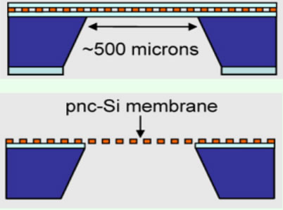
Using ethylenediamine pyrocatechol, or EDP, a huge amount of material is etched from the silicon wafer along crystal planes. This process leaves the membrane stretched approximately 500 microns across a square opening in the silicon wafer. Because the crystals in the membrane have random orientations, the membrane is extremely strong.
Buffered oxide etchant is used to strip the protective oxide layers from the freely suspended ultrathin porous nanocrystalline silicon (or Pnc-Si) membrane. Because the resulting holes are defined by the silicon crystal planes, they are shaped like pyramids with extremely smooth sidewalls, allowing the molecules propagate very easily through it to the membrane with essentially no loss.
Images--Top, material has been etched from the silicon wafer. Bottom, the oxide has been removed from both sides of the membrane, leaving an extremely strong yet flexible nano-membrane filter.
The ultrathin porous nanocrystalline silicon membrane can withstand a lot of pressure. The research team applied as much as fifteen pounds of pressure per square inch, or one atmosphere of pressure, to the membranes. And while the membranes bulged a bit and stretched, they did not break. The remained stable and strong, and they continued to filter molecules rapidly with great precision.
Additional Details
For further details, see:
Christopher C. Striemer, Thomas R. Gaborski, James L. McGrath, and Philippe M. Fauchet, "Charge- and size- based separation of macromolecules using ultrathin silicon membranes," Nature, February 2007.
Lois Gresh