
2007 News Archive
Ballistic Electronics: Low-Power Room-Temperature Nanoscale Terahertz Transistors
For the past few years, ECE Professor Marc J. Feldman has been designing low-power Terahertz transistors using two-dimensional electron gases (2DEG) inside structures that are smaller than 100 nanometers in size. The room-temperature devices are known as ballistic deflection transistors (BDTs) because they bounce electrons off nano-deflectors to create digital output.
With his team, Feldman received substantial grants from the Office of Naval Research, the Air Force Office of Scientific Research, and the National Science Foundation (NSF). The NSF "Nanoscale Interdisciplinary Research Team" grant was awarded in August 2006 for 1.1 million dollars. Preliminary results showed that the group's new BDTs should generate very little heat and require very low power. In addition, they can be fabricated using current technology.

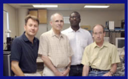
Professor Marc J. Feldman (group photo, top right) coined the term, ballistic electronics, and spearheaded a research team consisting of: (group photo, left to right) Martin Margala (ECE circuits), Yonathan Shapir (Physics Dept.), Paul Ampadu (ECE architecture), and Feldman (ECE device scientist). Key team member Quentin Diduck (left) received his ECE PhD in May 2007.
The ballistic model ranges back to the 1980's. For example, in 1989, C.W.J. Beenakker and H. van Houten published a Physical Review Letters paper called "Billiard Model of a Ballistic Multiprobe Conductor," which described a classical model of ballistic transport where electrons bounce around like billiards. Professor Feldman started thinking about ballistic electronics, a term he coined, realizing that classical physics doesn't quite explain what's happening when we move into the quantum-mechanical realm where electrons are tightly confined within nanostructures.
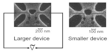
Even more intriguing, ECE graduate student Quentin Diduck focused on results published during the past decade about non-linear room-temperature ballistic rectifiers. In the displayed example (Reference: Song et al., Jpn. J. Appl. Phys. 40, L909, 2001), the device runs a small-amplitude AC current back and forth across a 100 or 200-nanometer device, producing DC voltage from top to bottom as the electrons hit the dark center obstacle. The 2DEG is shown in gray and is confined to a nano space. When the electrons hit the center obstacle, they are deflected downward.
Current Ballistic Electronics at the University of Rochester
The group is now working to further the progress made by researchers such as Song in 2001. For instance, Diduck added gates to Song's ballistic rectifier, thereby turning it into a transistor. As electrons are accelerated from bottom to top, the small gate voltage steers the electrons to one or the other side of the deflector obstacle. Other BDT geometries are under study as well. In addition to creating a new ballistic deflector transistor, the group is working to define an architecture for assembling these nano-sized devices into circuits. And their simulations demonstrate that the devices should operate with low power at TeraHertz frequency, thus facilitating the design of an ultra-high rate of analog-to-digital conversion.
The Rochester team fabricates its devices at the Cornell Nanofabrication Facility (CNF). In the photo (below left), the gray areas are the 2DEG, and the tiny triangle in the middle is the obstacle off which the electrons bounce. This device is pushing the limits of current-day fabrication of small structures in these materials. A variety of other elementary designs have been fabricated and tested, and show nonlinear ballistic transport at room temperature.
The typical mean free path of conduction electrons in a good metallic conductor is 5-20 nanometers; for the 2DEG used at 300 K, it is 100-200 nanometers -- much longer mean free paths than obtained with metallic conductors; and for some 2DEG at 4 K, it ranges from 1 to 10 micrometers, much longer still.
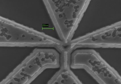
The narrow channels confine the 2DEG into a one-dimensional flow to yield long mean free paths and low electron collision levels. The green space bar is 250 nanometers long.
In a perfect metal the electrons would travel ballistically, without any collisions. The short mean free path of a real metal implies that the electrons collide frequently with impurities, grain boundaries, dislocations, and phonons. But if the mean free path were extremely long, and only a few collisions occured, then Ohm's Law,
I (current) = V (voltage) / R (resistance)
would break down. The resulting classical equation would be:
I (current) ~ square root of V (voltage)
But this classical result does not occur. Rather, in the accepted model of nano-level ballistic electron transport provided by the Landauer-Buttiker Theory, current travels as if it's in an electron waveguide. That is, the electrons are waves and the electron wavelength is quantized inside the transverse dimension of the channel. At this point, we are no longer in the classical realm; rather, we are in the quantum mechanical realm and dealing with energy levels. This is usually observed only at very low temperatures.
Think of the electron waveguide of a certain width as a string that can oscillate in three possible ways:
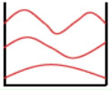
Because each electron has two spins, up and down, there are actually six possible modes for this system in the transverse dimension. These oscillations are extremely fast, producing what is basically quantized conductance is
e2 / h = 1 / (12,400 Ω) per oscillation mode
h / e2 = 12,400 Ω
It is shocking to some that the resistance of a ballistic channel does not depend upon how long the channel is -- it only depends upon how wide it is.
The Future of Electronics: Nano-Circuitry
With semiconductors, dopants are used to increase conductivity, but once the electrons are traveling, they can also collide with the dopants and scatter. If the doping is increased, the scattering increases, and as noted above, the mean free paths aren't particularly long.
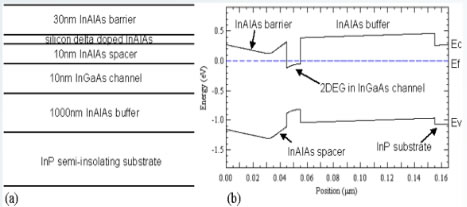
To avoid the doping problem, Professor Feldman's group uses a nano-device that confines the dopants to one layer. In the drawing below, that layer is identified as "silicon delta doped InAIAs," with InAIAs representing Indium Aluminum Arsenide. Notice the 10-nanometer InAIAs spacer between the dopant layer and the 10-nanometer Indium Gallium Arsenide (InGaAs) channel, where the 2DEG resides. The electrons are attracted to the InGaAs and jump down to that channel from the dopants. The electrons in the InGaAs channel travel without hitting the dopants because the 2DEG and the dopants are physically separated by the field in the 10-nanometer InAIAs spacer. That's why the mean free path in the 2DEG, even at room temperature, can be so long -- in fact, longer than the size of the nanostructure in the BDT.
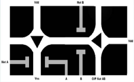
By combining multiple BDTs, Professor Feldman's team is building simple prototype circuits. One example is a logical NAND gate created from two ballistic deflector transistors:
Approximately one year into their four-year NSF grant, the team is just beginning to explore ballistic nano-architectures. Soon, we may be turning in our PCs and Macs for TeraHertz nano-computers with ballistic speed.