Author: Tian Qiu, Qiang Lin
Abstract
Thin-film lithium niobate (TFLN) has recently emerged as a pivotal material platform for high-performance photonic integrated circuits (PICs), primarily due to its exceptional electro-optic properties, wide transparency range, and potential for advanced integration. While current designs focus predominantly on the telecommunications band, there is a pressing need to adapt these technologies to the visible spectrum. This thesis investigates the design of an inverse taper edge coupler for the visible band (specified on 632.8nm), leveraging lithium niobate’s unique properties and optimizing coupling efficiency using the Lumerical Finite Difference Eigenmode (FDE) solver and the EigenMode Expansion (EME) solver. Simulated 1-layer inverse taper design has -0.76 dB coupling loss, and the 2-layer structure has -1.22 dB loss. The Lumerical design is then fabricated and experimentally tested to evaluate its performance. For the first fabrication results, the experiment shows that input light experiences a large transmission loss passing through the waveguide. It may be because the output and part of the taper region are too thin and might be blown away during fabrication. And there is a large loss when entering the waveguide region due to a sharp change in size. A fabrication test is also done to see its limit. In future, the design will be further optimized according to the result.
Theory
The overall coupling efficiency comprises two key components: first, the mode overlap between the input fiber mode and the desired eigenmode (TE or TM) at the start of the inverse taper facet; and second, the transmission efficiency through the taper region. The overlap efficiency is defined as:
This equation measures the fraction of electromagnetic fields that overlap between the two field profiles (modes). This is also the fraction of power from mode 2 that can propagate in mode 1 (for both forward and backward propagating fields).
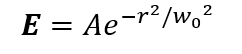
The target single-mode fiber for coupling analysis has an operating wavelength of 632.5nm with 2um spot size. Its near-field distribution of the fundamental mode is well-approximated by a Gaussian function.
Simulation Results
Here is the overlap efficiency between the fiber fundamental mode and the taper fundamental TE mode by scanning the width and height of the tip size of the taper:
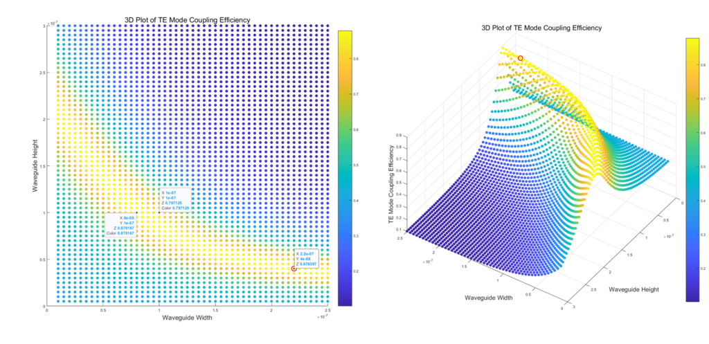
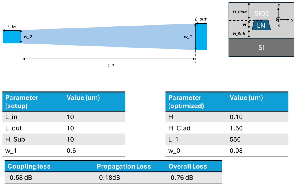
Initial Design: Single Layer
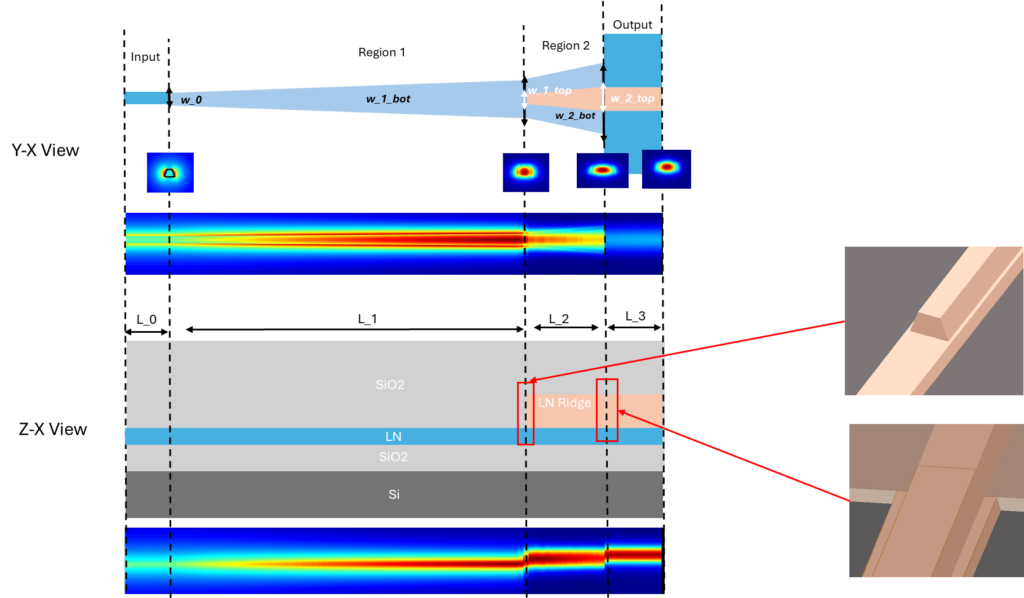
Improved Design: Bi-Layer
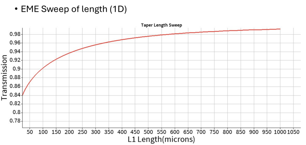
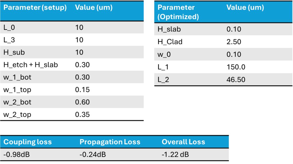
Although a 550 µm taper is relatively enough, it is still too long for a on-chip edge coupler design. Besides, the tip taper size is too small, which is only 80nm. It increases the difficulty of fabrication significantly and is hard to realise. As a result, an alternative inverse taper design is presented to increase the fabrication success rate as well as keep the device short. Also, the double-layer structure is more applicable, as in most research, the waveguide we used on integrated photonics chips is a rib waveguide, which has two layers (A slab waveguide with a rectangular waveguide on top of it).
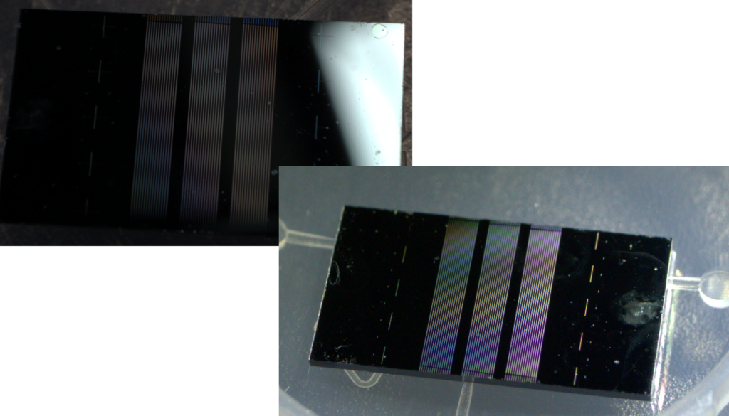
Fabrication Plan for Testing
With the help of the Ph.D students, Shixin Xue, Yueteng Zhang and Zhengdong Gao from Professor Qiang Lin’s research group, the design of bi-layer taper devices is fabricated for further testing.
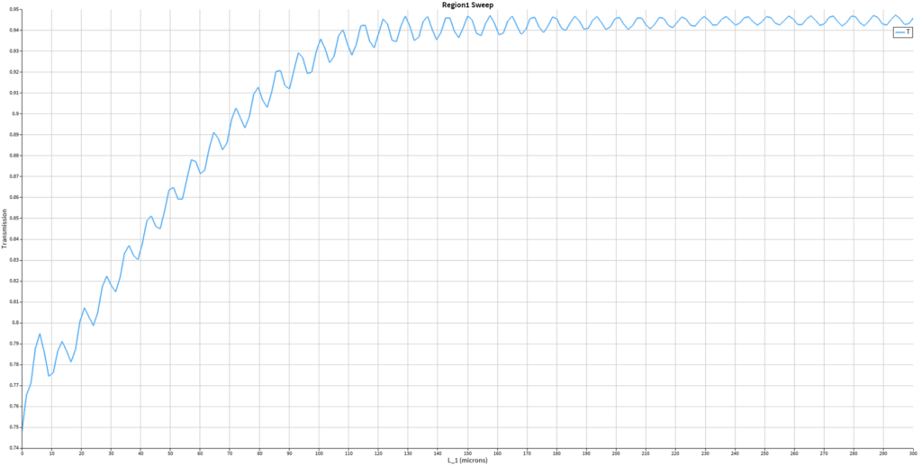
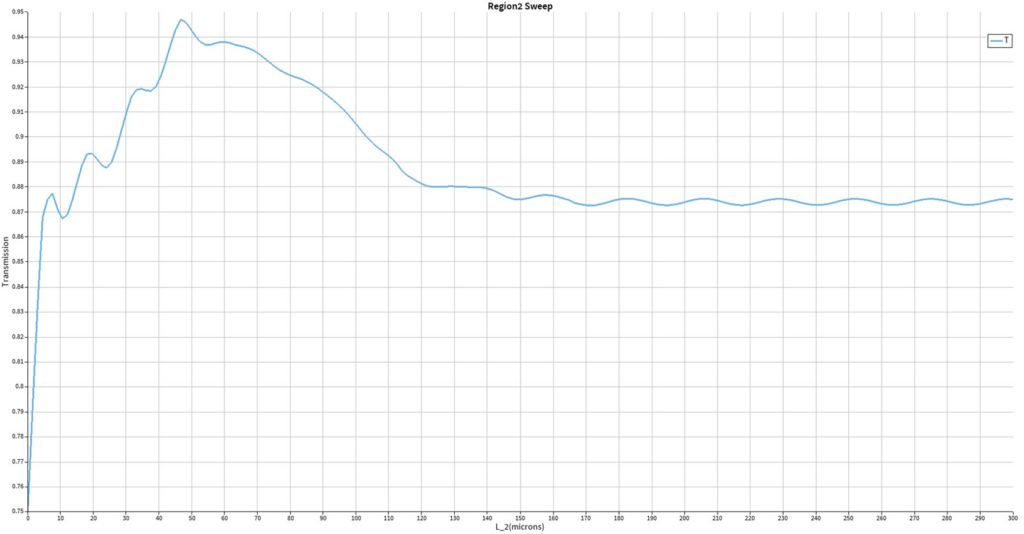
In total 45 device, for double Layer Design:
•1: Scanning L2 from 30um-100um, 15 points
•2: Scanning L1 from 80um-150um, 15points
•3: Scanning w_0 from 80nm-150nm, 15points
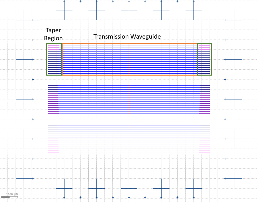
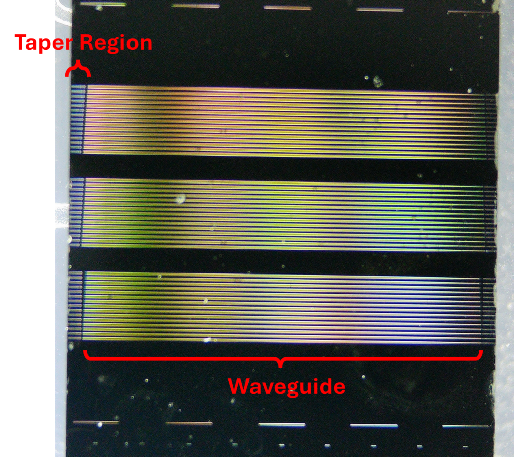
Testing and Results
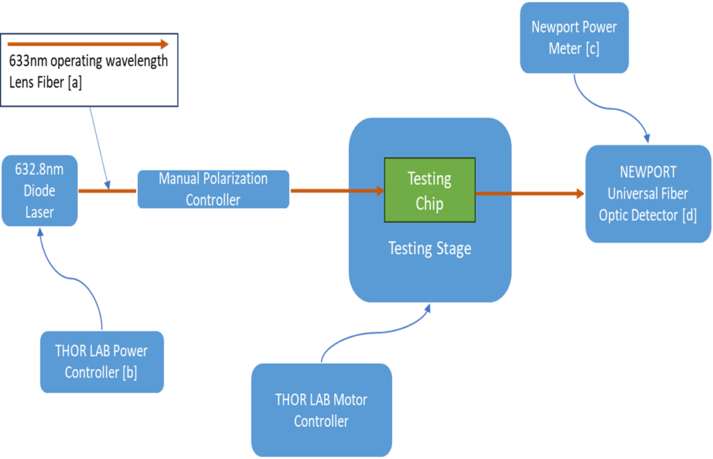
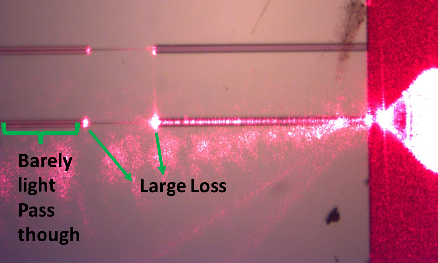
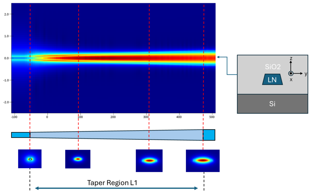
For the first fabrication results, experiment shows that input light experiences large transmission loss passing thought waveguide. From the figure there is barely light inside the untaped waveguide region.
It is may because the output and part of the taper region is too thin and might be blown away during fabrication. And there is large loss when entering the waveguide region due to sharp change in size. The design will be further optimized according to the result
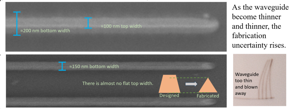
Fabrication Limits
Acknowledgement
I would like to express my heartfelt gratitude to Professor Qiang Lin for providing me with this invaluable opportunity to engage in real academic research under his guidance and support. I am also deeply grateful to Professor Knox for his advice and encouragement throughout the development of this proposal. Finally, I extend my sincere thanks to the Ph.D. students, Zhengdong, Shixin, Yueteng, and Chili in Professor Lin’s research group for their fabrication assistant, valuable suggestions and feedback on this research.
References:
- Liu, X. et al. Ultra-broadband and low-loss edge coupler for highly efficient second-harmonic generation in thin-film lithium niobate. Adv. Photonics Nexus 1, 016001 (2022).
- Ying, P. et al. Low-loss edge-coupling thin-film lithium niobate modulator with an efficient phase shifter. Opt. Lett. 46, 1478–1480 (2021).
- Zhu, D. et al. Integrated photonics on thin-film lithium niobate. Advances in Optics and Photonics. 12, 1415 (2021).
- Li, Z. et al. Silicon nitride assisted tri-layer edge coupler on lithium niobate-on-insulator platform. Opt. Lett. 48, 3367–3370 (2023).
- Liu, G. et al. Low-loss and broadband polarization-diversity edge coupler on a thin-film lithium niobate platform. Opt. Lett. 48, 4145–4147 (2023).
- He, L. et al. Low-loss fiber-to-chip interface for lithium niobate photonic integrated circuits. Opt. Lett. 44, 2314–2316 (2019).
- Guo, Z. et al. Polarization-insensitive and high-efficiency edge coupler for thin-film lithium niobate. Opt. Lett. 49, 2537–2540 (2024).
- Boes, A. et al. Lithium niobate photonics: Unlocking the electromagnetic spectrum. Science 379, eabj4396 (2023).
- Xue, S. et al. Full-spectrum visible electro-optic modulator. Optica. 10, 125–126 (2023).
- Mode Field Diameter of a Single-Mode Fiber. Indian Institute of Technology Roorkee – Laser Physics Laboratory. PDF document (Accessed: 5 December 2024).