Team
- Sirui Tang
- Yi Wang
- Yuning Xia
- Jingkai Ye
Mentor
- Parag Kelkar (ASML Customer)
- Jennifer Kruschwitz (Faculty Advisor)
Abstract
The desired product is a thin-film model used to predict the index profile and simulate the optical performance of plasma-etched nanostructure AR coatings. Our goal is to develop thin-film coating models using OptiLayer, OptiChar, and OptiRE based on observed microscopic geometrical structures of each sample surface and strive to closely match measured performance data from ellipsometer and spectrophotometer. We then aim to use the fitted thin-film models to investigate how parameter change in the etching process affects the index profile and performance of the manufactured samples.
Introduction
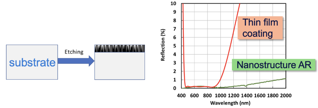
Nanostructure coating is a new kind of coating without actually coating any materials on the glass surface. Instead, it removes material from the glass surface to create nanostructures. By mixing substrate material and air under nano-scale, it creates the same effect as different indices. Compared with traditional thin-film coatings, nanostructure coatings can work for a wider bandwidth from UV to IR.
Background
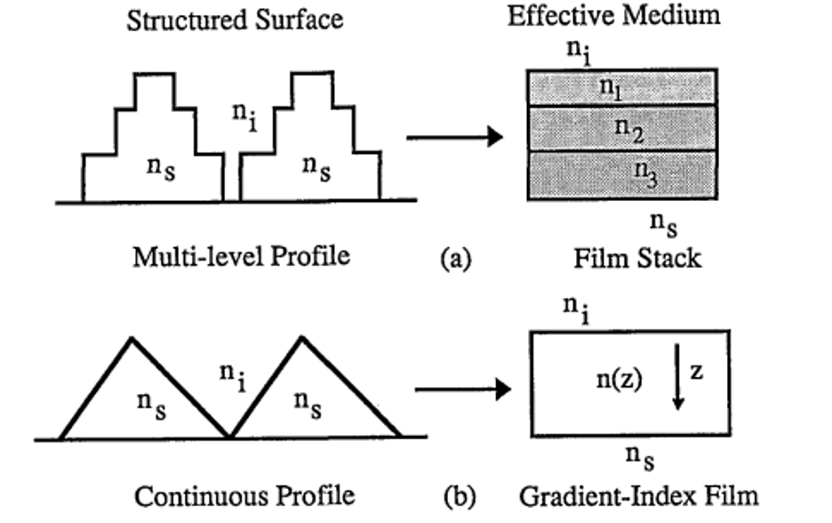
Nanostructure coating produced from the etching process has a periodic subwavelength pattern. When light interacts with these structures, it will not diffract as if it interacts with a diffraction grating. Instead, it will reflect and transmit as if it encounters a medium [2]. Effective medium approximations (EMA) could be applied to describe these phenomena. In general, the optical properties of the effective medium are like the weighted spatial average of the profile region’s optical properties [2]. Figure 2 below shows two examples of nanostructure profile shapes and their effective medium approximation. For a multi-level surface relief profile (Figure 2.a), the effective medium is a film stack where each layer of the film stack corresponds to a distinct level of the surface-relief profile. For a continuous profile (Figure 2.b), the effective medium is a gradient film.
In this project, we use SEM to observe the profile of the sample. With the geometric structure of the profile, we can determine its effect medium approximation, which helps to establish the starting point of our thin-film model. The starting point is a combination of film stacks and gradient films based on the structure we observe. The index of air and the substrate is known, so the index for the mid-layers can be fitted by each sample’s optical performance, such as the ellipsometry and spectrophotometry data.
Measurements
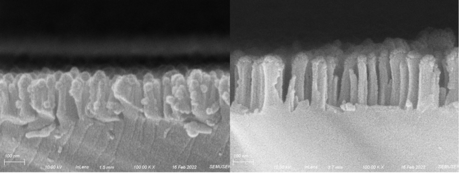
SEM pictures of the cross-section profile of the samples.
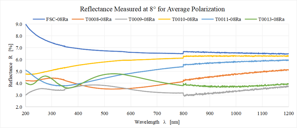
Reflectance measured at an incident angle of 8° for average polarization.
Ellipsometry data measured at incident angles from 45° to 75°.
Modeling
By looking at the SEM pictures that show the geometrical shape of the nanostructures on the sample surfaces, we can build either single-layer or multi-layer models with both mixture material and inhomogeneous materials. This process involves a lot of trial and error because from the side profile pictures, we have many options as to how to divide the layers up and whether inhomogeneity is needed or not for each.
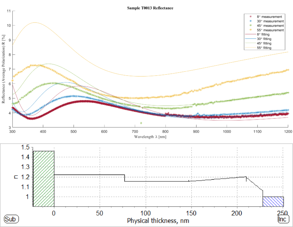
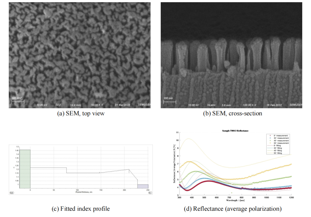
For example, the following sample (T0013) has a clear side profile from the SEM. We can estimate the shape as two trapezoids on top and two rectangles on the bottom. In this way, the roughly estimated index profile based on the structure is shown in Figure 3.
As shown, the model we have for this sample has four layers, where the bottom two are made of mixed materials of the substrate and air, which have fixed indices. The top two layers are also made of mixed materials but with inhomogeneity applied because their structures are not uniform as the physical thickness increases. The layers that have inhomogeneity have increasing or decreasing indices that start from where the layer before it ends, and end at where the layer after it starts. The fitted reflectance data at different incidence angles and the index profile of the model are shown in Figure 4.
The models for all the samples are folded below. Generally, for the under-etched samples, we focus on simulating reflectance, ellipsometric data, and etched thickness using single-layer models. For the well-etched samples, we focus on simulating the cross-section structure and reflectance data using multi-layer models with inhomogeneities.
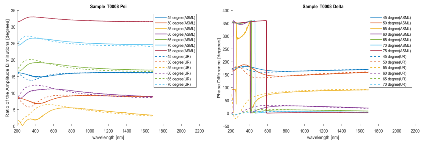
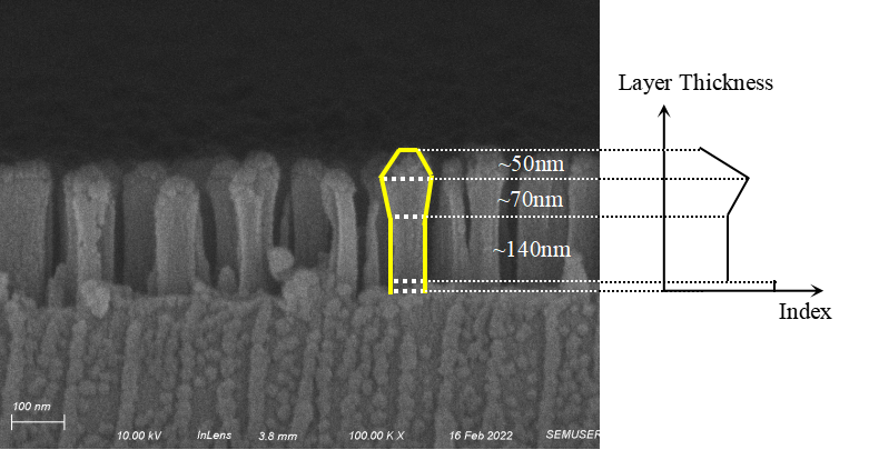
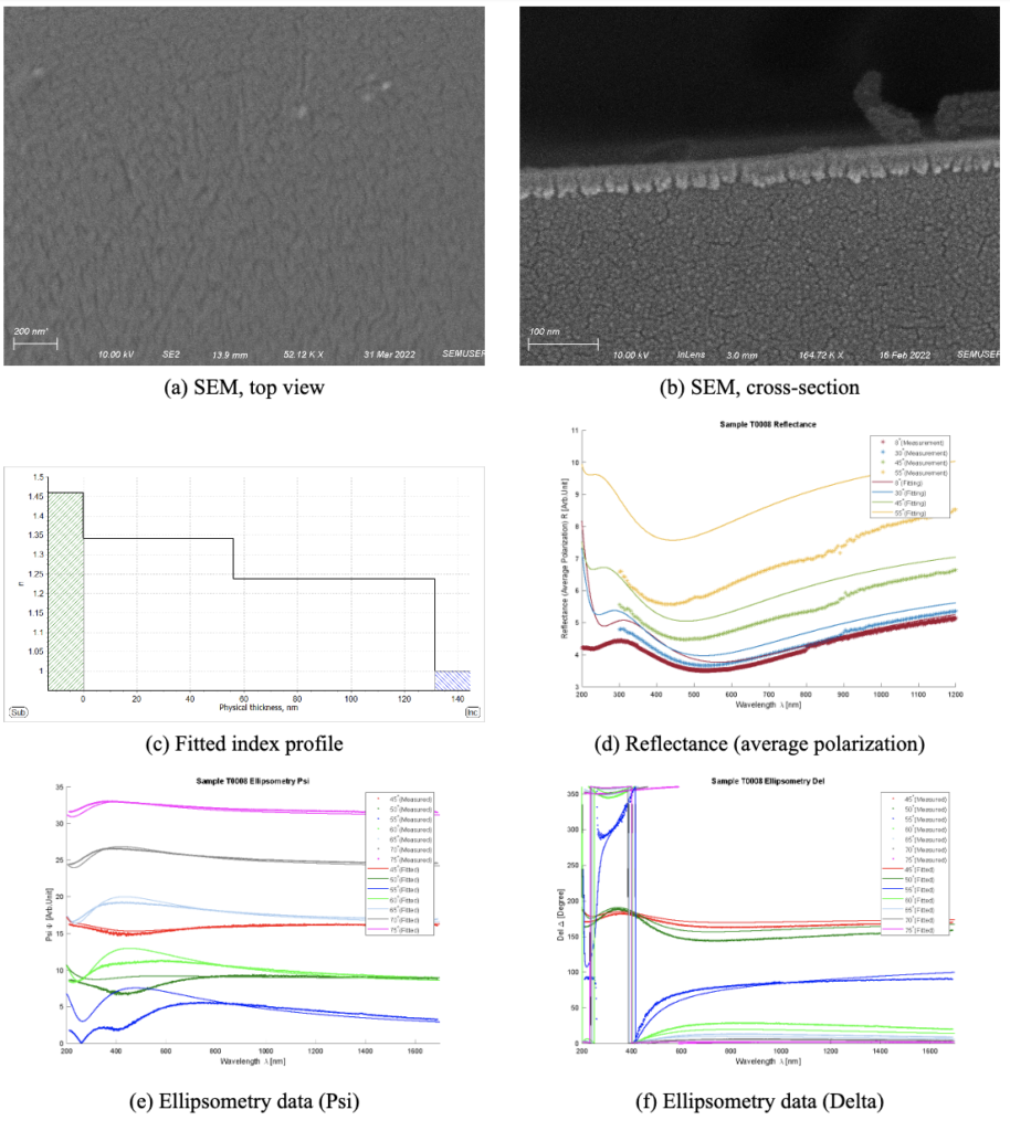
Layer model for Sample T0008
The final fitting result for sample T0008 is a two-layer model.
- First layer: a mixture of 75% of substrate glass and 25% of air. Thickness of 56.173nm.
- Second layer: a mixture of 53.09% of substrate glass and 46.91% of air. Thickness of 75.269nm.
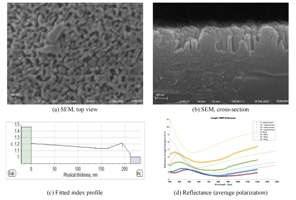
Layer model for Sample T0009
The final fitting result for sample T0009 is a four-layer model with inhomogeneities.
- First layer: a mixture of 40% substrate glass and 60% of air. Inhomogeneity of -6%. Thickness of 137.679nm.
- Second layer: a mixture of 30% substrate glass and 70% of air. No inhomogeneity. Thickness of 27.413nm.
- Third layer: a mixture of 40% substrate glass and 60% of air. Inhomogeneity of 6.5%. Thickness of 30nm.
- Fourth layer: a mixture of 30% substrate glass and 70% of air. Inhomogeneity of -15%. Thickness of 17nm.
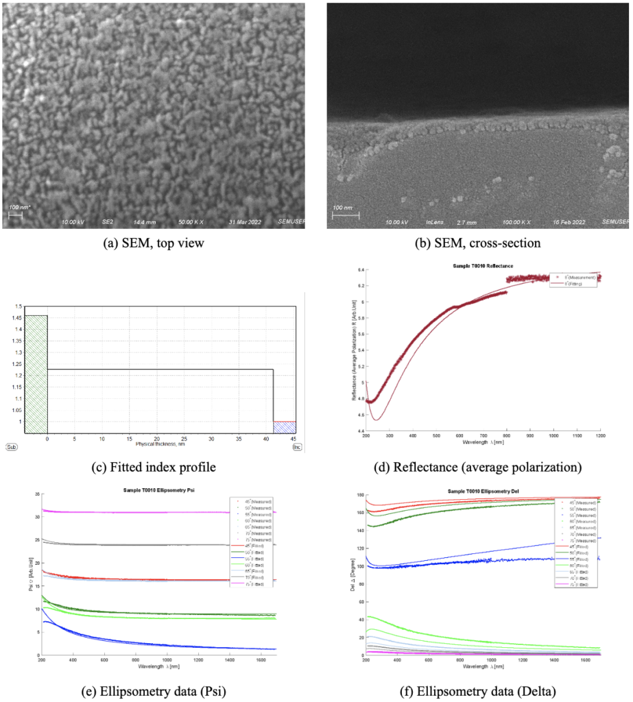
Layer model for Sample T0010
The final fitting result for sample T0010 is a single-layer model, which is a mixture of 50.81% of substrate glass and 49.19% of air with a thickness of 41.319nm.
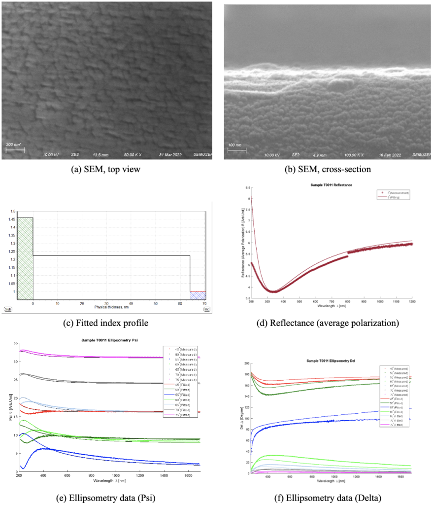
Layer model for Sample T0011
The final fitting result for sample T0011 is a single-layer model, which is a mixture of 50% of substrate glass and 50% of air with a thickness of 64.112nm.
Layer model for Sample T0013
The final fitting result for sample T0013 is a four-layer model with inhomogeneities.
- First layer: a mixture of 50% substrate glass and 50% of air. No inhomogeneity. Thickness of 77nm.
- Second layer: a mixture of 35% substrate glass and 65% of air. No inhomogeneity. Thickness of 68.891nm.
- Third layer: a mixture of 40% substrate glass and 60% of air. Inhomogeneity of 4%. Thickness of 63nm.
- Fourth layer: a mixture of 30% substrate glass and 70% of air. Inhomogeneity of -12%. Thickness of 18nm.
Conclusion and Acknowledgment
We have developed multi-layer thin-film coating models that both carefully reflect the geometry of the nanostructure and closely simulate the sample’s coating performance. We expect the models to help ASML to investigate how parameter change in the etching process affects the index profile and the optical performance of the manufactured samples, and therefore improve the technique.
We greatly appreciate the technical advice from Prof. Jennifer Kruschwitz and the support from Prof. Brian McIntyre (URnano), Dr. Amy Rigatti (LLE), Ni Huo (Chemistry Department), and Prof. Wayne Knox.
References
[1] Parag Kelkar. “Nanostructure Anti-reflection Coating Characterization,” lecture notes, (2021).
[2] Daniel H. Raguin and G. Michael Morris, “Antireflection structured surfaces for the infrared spectral region,” Appl. Opt. 32, 1154-1167 (1993).