A Slow “Macro-Processor” for Education and Demonstration
Team Members
Benjamin C. Heyman
An Ho
Supervisors
Jack Mottley, PhD, Electrical and Computer Engineering, UR | Daniel Phinney, Adjunct Faculty, Electrical and Computer Engineering
Customers
N/A
The Problem
ProcBlocks is an educational tool designed to introduce students to the basics of computer organization. College programs in Computer Engineering often include an “Introduction to Digital Logic” course, which serves as a prerequisite to a “Computer Organization” course. The intention is to provide students with an understanding of what can be done with digital logic, the typical tricks used to implement certain functions, and the difficulties that arise from this type of computing. This motivates the discussions in Computer Organization about pipelining, clock speeds, parallelizing, and so on. In the late 20th century, this discussion would also rely on experience: many students would have interacted with low level computers like the Commodore 64 or Apple II, affording them a sense of memory and machine instructions. However, in the modern day of fast microprocessors, many students are left without that “feel” for how computers work, or a sense of how digital logic and computer organization are related. What we need is to turn back time, and provide students with a practical application of the concepts learned in digital logic without going all the way to 5-stage pipelined processors. This project therefore aims to create a slow, macro processor where each component can be studied individually. An accompanying text would walk students through each digital logic concept and then introduce it practically on the ProcBlocks hardware.
The Concepts
The goal of the ProcBlocks project is to be versatile. The hardware is successful if it lends itself well to many different lessons. This is a small set of lessons that could be taught using the ProcBlocks hardware:
- Bitwise Operations
Bitwise operations are one of the most valuable tools in low-level programming. The effect, however, is often lost on those who have only experienced variables in integer/floating-point formats. Accordingly, using the arithmetic logic unit (ALU) block and two input blocks, a lesson could be taught about the effects of different bitwise operations. For instance, the masking properties of AND, the joining properties of OR, and the selective inverting properties of XOR.
- Memory
Reading and writing to memory can be demonstrated through the use of the clock block, an input block, and the data memory block. Students could write information into data memory and then attempt to retrieve each other’s data.
- Busses
Busses are an often misunderstood portion of digital logic. By making use of two register blocks, an ALU, and a single input block, the value of using a common bus can be demonstrated.
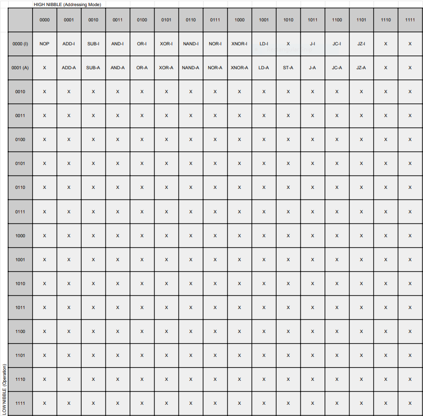
The Instruction Set Architecture (ISA)
The goal in designing the ProcBlocks ISA was threefold: (1) create something Turing complete (2) only use the most basic operations (3) make it easy to only use a subset of the ISA. Accordingly, we adopted a convention similar to the 6502 processor. The high-nibble of the 8-bit opcode specifies the addressing mode, while the low-nibble specifies the operation. Accordingly, leaving out addressing modes is as simple as restricting the high nibble to certain bits or bit patterns. Due to time restrictions, we have only included an “immediate” addressing mode and a “direct” addressing mode. The rest are left as open spaces for further ISA expansion.
The Hardware
The hardware modules will be listed below, along with a schematic diagram. The modules are listed in the order that they are most naturally introduced, along with a brief explanation of how the block can be added. Note that both input blocks and a power block are needed, but not shown, as they do not include any digital logic.
- The Clock Block
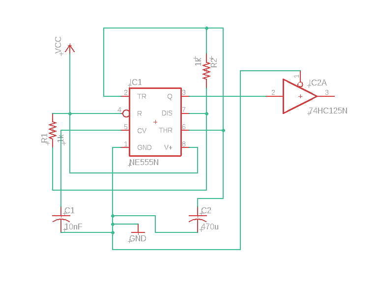
This block is the only component that makes use of analog circuitry. Accordingly, its design is not something that would be studied. The relevant discussion around clock cycle, frequency, duty cycle, rise time, and fall time could occur at this point. It may also be possible to include some small discussion about the analog components, if time permits. After reviewing the relevant concepts, this block is abstracted as a 1 Hz clock signal.
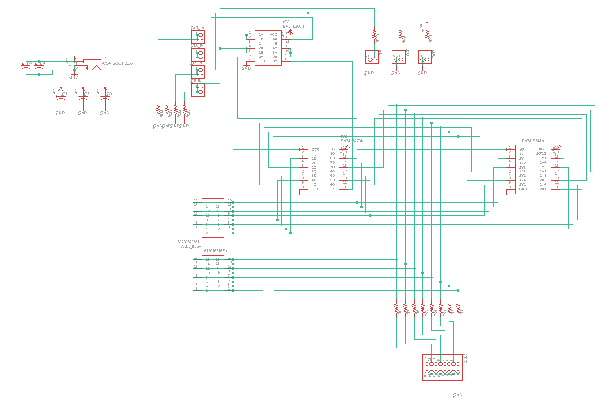
- The Arithmetic Logic Unit (ALU)
This block allows for arithmetic and logic operations to be executed on two 8-bit values. The operation is selected by three select signals. At this point, two input blocks could be used to demonstrate the functionality of the ALU and its relevant components would be discussed in detail (for instance, multiplexores, decoders, tri-state logic, etc). The ALU implements ADD, SUB, AND, OR, XOR, NAND, NOR, XNOR and includes two status bits: zero and carry.
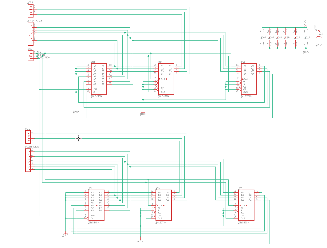
- Register
The register is the first introduction of a synchronous component. The register stores the 8 bit value at its input when enabled and receiving a positive clock edge. The register can also produce a high impedance output or the data output depending on a select signal. This component would be used to introduce D-flip flops and could be connected as inputs to the ALU to allow for the use of a single input block and a common data bus.
- Instruction Memory

This block would be the introduction of memory; specifically, the instruction memory makes use of an electrically erasable programmable read-only memory (EEPROM). Students would therefore gain experience in writing to a nonvolatile memory and reading from said memory. This could first be done with an input block and later with an Arduino program.
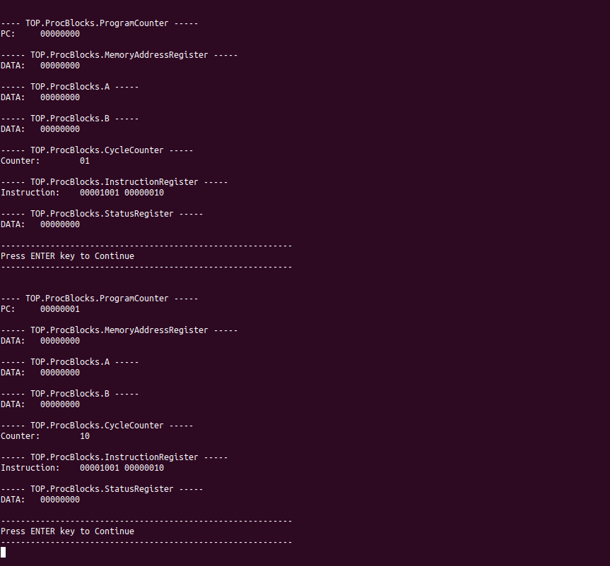
- Instruction Register
The instruction register is similar in function to the regular register, but holds 16 bits, which is the width of an instruction. No further information is necessary to add this block.
- Program Counter (PC)
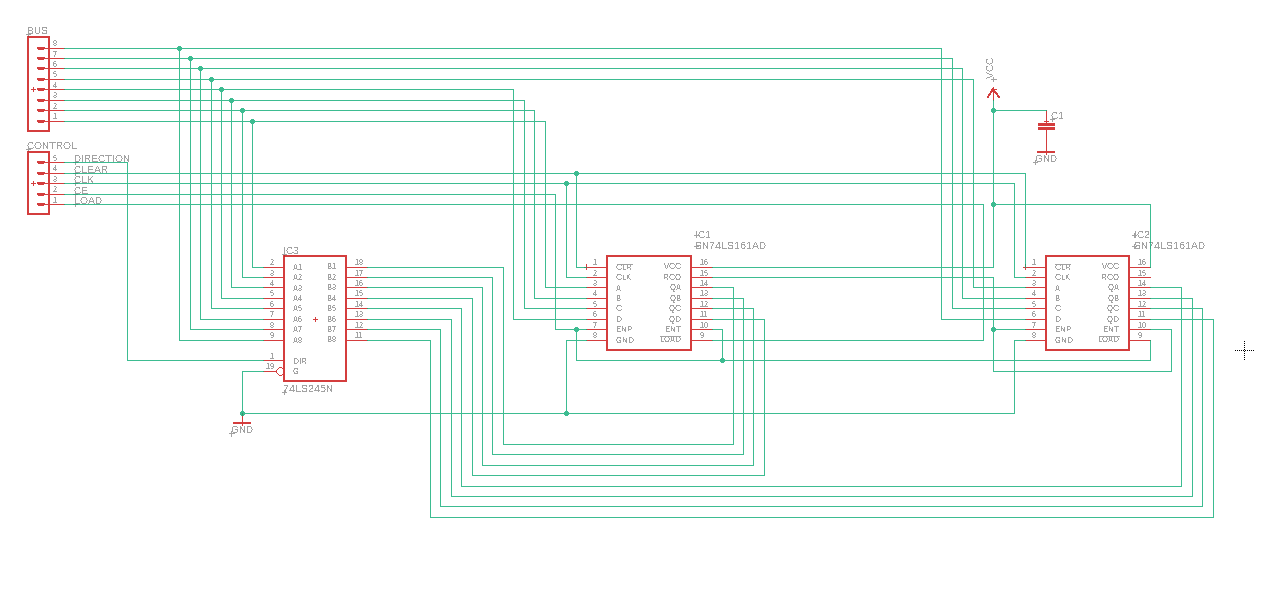
The program counter is used to address instruction memory and introduces the concept of incrementing. Once again, this block can be demonstrated using the clock block and an input block.
- Data Memory
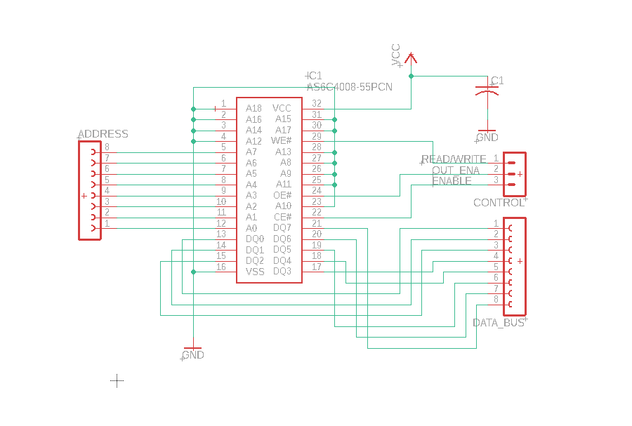
Data memory is similar to instruction memory, except that it is writable and volatile. This block would introduce these two concepts and could be used individually with a clock block and an input block.
- Decoder

The decoder is the last component introduced. Its function could be replaced initially with a student who would read the opcode and determine the necessary control signals, which would be set with an input block. The decoder then provides a very satisfying way of simplifying and automating this process, culminating in a fully working processor.
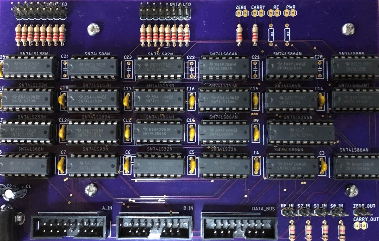
All the hardware components can be designed in printed circuit board (PCB) similar to the ALU. They can then be connected together to represent the processor. The Instruction memory is made by EEPROM so that it can be programmed to test the hardware. An assembler is written to translate the assembler code from the ISA to binary files that can be stored in the instruction memory. For future improvement, more Light-emitting diode (LEDs) and Liquid-crystal display (LCD) can be added to the system to monitor the output of the processor and help mitigate the learning process.