Kunyang (Benny) Cao, B.S. Optics 2026
Advisors:
Professor Pablo A. Postigo, Christer Everly
1. Abstract
Low threshold laser is desired to reduce power consumption and minimize the thermal load in integrated photonics. One-dimensional photonic crystal cavity, or nanobeam, has been shown to be a good candidate for low threshold laser’s cavity due to its ultra-high cavity quality factor. In this work, an existing nanobeam design made of GaAs is used as the starting point of my design and is then optimized in COMSOL for a higher quality factor. The nanobeam’s geometrical structure, specifically its air holes’ taper profile, is optimized through novel methods of optimization, namely parameter optimization and genetic algorithm. The manufacturability of the nanobeam is also evaluated by simulating different amounts of air hole radius sizing errors during fabrication.
2. Background and Theory
In semiconductor laser, spontaneous emissions that are not contributing to the lasing forms the lasing threshold. A laser with low threshold or even close to zero threshold is what optical engineers seek [1]. One-dimensional photonic crystal cavity, or nanobeam, has demonstrated a high quality(Q) factor and small mode volume (V_m). Those two characteristics enhance the spontaneous emission rate of the emitters through Purcell enhancement, which states that the spontaneous emission rate is proportional to Q/V_m, therefore decreasing the laser threshold [2].
Nanobeam is a photonic crystal cavity that has periodic structure only in one dimension, as shown in figure 1. Geometrical parameters such as the cavity length L_c, nanobeam width w, periodicity p, air hole radius r can describe the structure of the nanobeam well and makes it easy to optimize for a larger Q-factor.
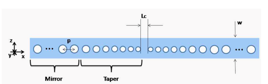
Fig. 1. A schematic of a nanobeam [3]
3. Method
Finite Element Method (FEM) will be the simulation method we used to obtain the electromagnetic distribution and quality factor in a nanobeam resonator, and COMSOL will be the software to use. A typical framework of simulation is shown in Figure 2. The outer rectangle is defined so that scattering boundary conditions are applied at the boundary. This boundary condition makes the outer rectangle nearly non-reflective for the light reaches it, eliminating any “artificial” recovery of lost energy. The starting point of the optimization is adapted from the nanobeam designed by Gong et.al [4].
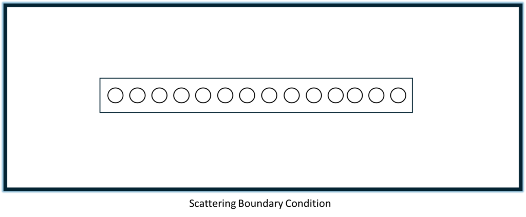
Fig. 2. Paradigm of nanobeam simulation in COMSOL.
Parameter Optimization and Genetic Algorithm are the two methods of optimization being used in this thesis. Parameter Optimization is a COMSOL built-in non-gradient optimization methods. Genetic Algorithm, in another hand, is an optimization method that is inspired by evolution. Since COMSOL doesn’t have a built-in genetic algorithm in its optimization module, a self-written genetic algorithm code in MATLAB is required to control the COMSOL to perform genetic algorithm optimization. How MATLAB and COMSOL is communicated is shown in Figure 3.
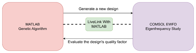
Fig.3. A flow chart demonstrating the communication between MATLAB and COMSOL
4. Results and Discussions
The taper profile of the nanobeam is very important for ultra-high Q-factor cavity. To preserve the quadratic taper profile, the taper profile is parametrized using the following two functions.
R(n)=An^2+Br_0
A(n)=Cn^2+Da_0
, where n is the numerical order of the air hole counted from the center, r_0 and a_0 are radius and periodicity of the air hole at the center. Parameter optimization and genetic algorithms are run to optimize [A,B,C,D,r_0,a_0] in 2D nanobeam simulation. After showing that those two optimization methods work in 2D, the parameter optimization method is run in 3D nanobeam simulation. The optimization results are shown in the following table and figures.
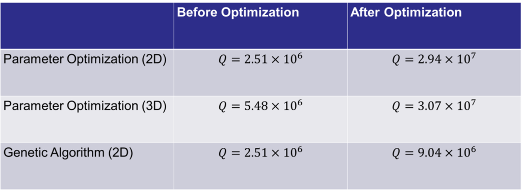
Table.1. The quality factors of three different optimization methods before and after optimization
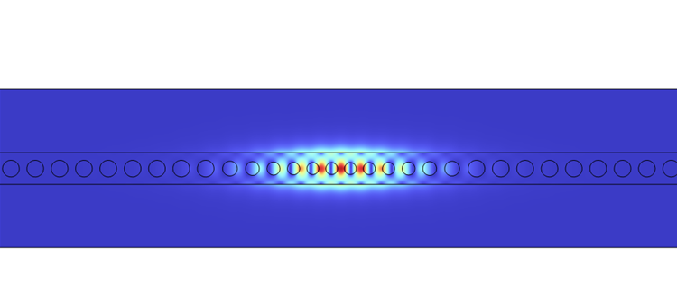
Fig.4. Electric field norm distribution after parameter optimization (2D Simulation)
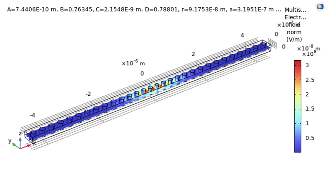
Fig.5. Electric field norm distribution after parameter optimization (3D Simulation)
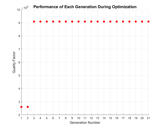
Fig.6. Quality factor of each generation during genetic algorithm optimization (2D Simulation)
In both parameter optimization and genetic algorithm optimization methods, the quadratic taper profile is essential to the nanobeam’s million-scale quality factor. Without parametrizing the taper profile using the two quadratic functions above, the taper profile is easily to break during optimization, generating a nanobeam with very low quality factor. In Figure 7, the air hole radius profiles of the original nanobeam and the optimized nanobeams with and without parametrizing in parameter optimization (2D simulation) is compared, along with their resulting quality factor.
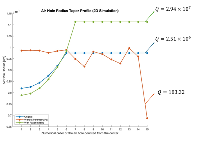
Fig.7. Air hole radius taper profile of the original nanobeam and the optimized nanobeams with and without parametrizing (2D simulation).
As in every engineering design, the manufactured nanobeam cannot have the exact performance as the designed nanobeam due to manufacture error. In Electron-beam lithography, typical manufacturing method of nanobeam, proximity effect is one of the primary sources of manufacturing error. The proximity effect states that forward-scattering and backscattering electrons cause undesired exposure at resist region adjacent to the exposed region, making the pattern size inconsistent with the design [5]. Here, I imitate the proximity effect to evaluate the manufacturability of the designed nanobeams. By multiplying each air hole radius a deviation factor, I simulate the air hole radius sizing error during fabrication. The deviation factor ranges from -5% to 5%, and the nanobeams’ quality factors and resonance wavelengths are reevaluated under the deviation factor, as shown in Figure 8.
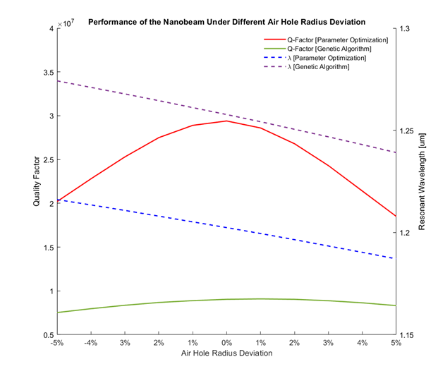
Fig.8. Performance of the optimized nanobeams (2D simulations) with different air hole radius deviation factors
It can be shown that a deviation factor within 5% didn’t drag both designs’ quality factors out of their order of magnitude. Compared to the change in quality factor of parameter optimized nanobeam, the change in quality factor of genetic algorithm optimized nanobeam is relatively smaller, indicating that the air hole radius of genetic algorithm optimized nanobeam is less sensitive to manufacturing error. Interestingly, the quality factor of genetic algorithm optimized nanobeam is higher with 1% deviation factor than with no deviation. This indicates that the genetic algorithm failed to find the locally optimized design within the specified generation number. Both design’s resonance wavelengths stay within of their original resonance wavelengths given the deviation factor is less than 5%.
5. Conclusion
In summary, this thesis proves the feasibility of optimizing nanobeam through FEM based classical optimization methods, namely parameter optimization and genetic algorithm. An existing nanobeam designed by Gong et.al. is used as the starting point for optimization. Parameter optimization in 2D electromagnetic wave frequency domain (EWFD) simulation increases the quality factor from 2.51*10^6 at resoance wavelength 1.30 um to 2.94*10^7 at resonance wavelength 1.21 um. Through introducing another dimension, the parameter optimization in 3D EWFD simulation increases the quality factor from 5.48*10^6 at 1.29 um to 3.07*10^7 at 1.25 um. Genetic algorithm was also applied to 2D EWFD simulation, and the quality factor obtained an increment from 2.51*10^6 at 1.30 um to 9.04*10^6 at 1.26 um. Both nanobeam designs maintain the same order of magnitude in quality factor and keep the resonant wavelength within 0.02 µm of the original value under a 5% manufacturing deviation in air hole radius.
6. Acknowledgement
I would like to express my appreciation to my advisor, Prof. Pablo A. Postigo, for his guidance and support throughout this project. His insights on the applicability of the optimized nanobeam in low-threshold laser provided tremendous motivation to me. His feedback on my manuscript were also invaluable.
I also wish to thank Christer Everly, Lukas Weituschat, and Jaymit Surve, especially Christer Everly, for helpful discussions and assistance about FEM simulation, FDTD simulation, and manufacturability of nanobeams.
Finally, I would like to thank my family and friends for their support and encouragement during the development of this thesis.
7. References
1. Susumu Nona. Seeking the ultimate nanolaser. Science 2006 Oct 13;314(5797):260–1.
2. Gu Q, Fainman Y. Semiconductor nanolasers. 1st ed. Cambridge University Press; 2017. .
3. Grande M, Calò G, Petruzzelli V, D'orazio A. High-q photonic crystal nanobeam cavity based on a silicon nitride membrane incor-porating fabrication imperfections and a low-index material layer. .
4. Gong Y, Ellis B, Shambat G, Sarmiento T, Harris JS, Vučković J. Nanobeam photonic crystal cavity quantum dot laser. 2010 -04-12.
5. Li P. A review of proximity effect correction in electron-beam lithography. 2015 -09-17.