ASML Reticle Contamination Inspection System
Team
Stephen Roberts
Frank Yin
Betty Li
Customer
ASML US, LLC
Customer Primary Contact
Matthew Scibilia
Project Advisors
Greg Schmidt
Oliver Zhai
Abstract
The ASML Reticle Contamination Inspection System project focuses on detecting contaminant particles on photolithography reticles used in semiconductor manufacturing. Reticles contain patterned features that transfer circuit information onto wafers during the lithography process. As a result, even small levels of surface contamination can degrade imaging performance, reduce yield, and impact overall device reliability.
However, current inspection approaches face a major challenge. Undesired ghost signals arise from reflections within the reticle structure, particularly from backside and patterned surfaces. These ghost reflections often overlap with the true signals produced by contaminant particles. Because of this overlap, inspection systems may incorrectly classify reflections as contamination, leading to false positives and reduced confidence in measurements.
To address this issue, we designed a scattering-based optical inspection system. Instead of relying solely on imaging resolution, this system focuses on separating scattered light from specular reflections. The final design improves discrimination between real contamination and optical artifacts while meeting the detection requirement for particles on the order of 10 µm.
Description
Deep ultraviolet (DUV) lithography relies on high-precision reticles to define nanoscale features on semiconductor wafers. These reticles consist of fused silica substrates with patterned structures that encode circuit information. During exposure, light passes through or reflects off these patterns to transfer the design onto a wafer.
Because of this process, reticle cleanliness is critical. Even relatively small contaminant particles can scatter light, distort the projected pattern, and introduce defects into fabricated devices. Therefore, reliable inspection systems play an essential role in semiconductor manufacturing.
At the same time, the optical behavior of reticles introduces additional complexity. Light interacting with the reticle does not follow a single path. Instead, it reflects from multiple interfaces, including the front surface, the patterned layer, and the backside of the substrate. These multiple reflection paths generate signals that can resemble contamination, which complicates detection.
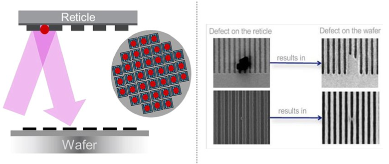
Figure 1. Illustration of multiple reflection paths in a reticle & how contamination signals can be confused with backside ghost reflections
The primary motivation for this project comes from the limitations of current inspection systems. In existing approaches, ghost reflections often mimic the appearance of real contaminant particles. These reflections arise from internal reticle structure and propagate through the optical system, eventually reaching the detector.
As a result, inspection systems may detect signals that do not correspond to actual contamination. This effect reduces detection contrast and increases false positive rates. In high-precision manufacturing environments, even small inaccuracies can have significant consequences.
Rather than simply improving spatial resolution, this project addresses the root cause of ambiguity. Specifically, the design focuses on distinguishing between different types of optical signals. The system identifies light scattered by particles while actively rejecting light produced by specular and backside reflections.
Scattering-Based Inspection Design
Figure 2. Left: reticle pattern. Right: contaminants detected by a previous inspection system showing ambiguity between real particles and artifacts
The final system concept uses a scattering-based detection approach. A line laser illuminates the reticle at an oblique angle so that directly reflected light follows a different path than light scattered by particles on the surface. The detector and collection optics are arranged to preferentially collect scattered light while avoiding the strongest specular reflection paths. This geometry helps separate true contamination signals from ghost reflections caused by the reticle structure.
The system design includes a 520 nm line laser source, a cylindrical lens for beam shaping, first-surface mirrors for folding and directing the optical path, Schneider SAPPHIRE line-scan lenses, Basler racer line-scan cameras, and a CMOS sensor. These components were selected to support a compact optical layout while maintaining enough signal level for particle detection. The design also considered source power, detector sensitivity, system volume, and optical path geometry.
System Architecture
The optical architecture was developed to reduce overlap between contamination-scattered light and ghost reflections. The illumination path directs a narrow laser line across the reticle surface, while the detection path collects light scattered away from the main reflected beam. This approach helps avoid collecting the strongest reflection from the reticle while still allowing particles to appear as detectable signals.
Figure 3. Conceptual layout and spatial constraints of the inspection system
A key part of the design was controlling the angles of illumination and collection. By choosing an oblique illumination geometry, the system increases the spatial separation between specular reflections and scattered contamination signals. This geometry is especially important because the reticle itself can produce structured reflected signals that may otherwise be mistaken for particles.
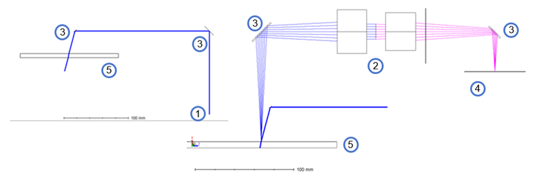
Figure 4. Left: detection geometry showing collection of scattered light. Right: illumination geometry showing oblique laser incidence on the reticle
System Performance
The designed system provides a physics-driven approach for reticle contamination inspection. Its main expected capability is the reliable separation of contaminant-scattered signals from ghost reflections. The design is intended to detect particles approximately 10 µm or larger while reducing false positives caused by unwanted reflections.
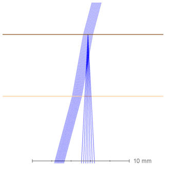
Figure 5. Key system components including line laser source, line-scan detector, and imaging optics used in the design
The system was evaluated through optical layout development, component selection, and analysis of how the illumination and detection geometry affects signal separation. The final concept emphasizes a practical scattering-based architecture that meets the customer’s design goals without relying only on high-resolution surface imaging. The result is a newly designed inspection solution that can be used as a foundation for future validation and performance testing.
Future Work
Future work will focus on experimental validation of the proposed system. Building a prototype and testing it with controlled contaminated samples will allow direct measurement of system performance. These tests will evaluate sensitivity, repeatability, and the effectiveness of ghost reflection suppression. Additionally, future efforts may optimize illumination geometry, detection angles, and source power. These adjustments can further improve signal-to-noise ratio and detection reliability.
Finally, additional studies may extend the system to detect smaller particles and different contamination types. Expanding the system’s capabilities will support broader applications and contribute to the development of scalable reticle inspection solutions.