Emily DeVeyra, Supervisor: Dr. Svetlana Lukishova
Abstract
In application to single (antibunched) photon sources (SPSs), we investigated a creation of photoluminescent centers in silver nanocubes, silicon nitrate (SiN), and a silicone-based contact lens hydrogel material under laser irradiation. Single-emitter confocal fluorescence microscopy, low-light spectroscopy, and a Hanbury Brown-Twiss correlator are used for characterization of laser-induced photoluminescence centers. Photon antibunching was observed from some of them in silver nanocubes treated by CW laser radiation at 405 nm and/or 532 nm as well as in femtosecond laser treated SiN.
Applications and Motivation
SPSs with photons exhibiting antibunching are nonclassical light sources with all individual photons separated in time [1]. SPSs have applications in quantum information, quantum metrology, and the biomedical field (antibunching super-resolution microscopy).We investigate the formation of new emitters for SPS applications by laser irradiation of different types of materials: semiconductor (SiN used in photonic integrated circuits), silver nanocubes (used in plasmonic nanoantennas), and a silicone-based contact lens hydrogel polymer (used in contact lenses). For instance, the defects induced by femtosecond laser irradiation promise close-to-atomic-scale laser manufacturing in solid-state substrates [2]. SPSs based on these defects with different fluorescence wavelengths (color centers) on the same substrate have been demonstrated by changing femtosecond laser irradiation doses.
At the same time laser-induced fluorescing centers can be harmful in plasmonic nanoantennas. Instead of enhancement of a single-emitter fluorescence through a Purcell effect, these induced fluorescing centers can compete with the main emitter preventing registration of its photon antibunching [3].
Fs laser irradiation of a contact lens polymer changes its refractive index and focusing of a contact lens. We investigate if this fs-laser treatment creates also fluorescing defects.
SAMPLES: fs-laser treated SiN, silver nanocubes, and fs-laser treated silicone based hydrogel
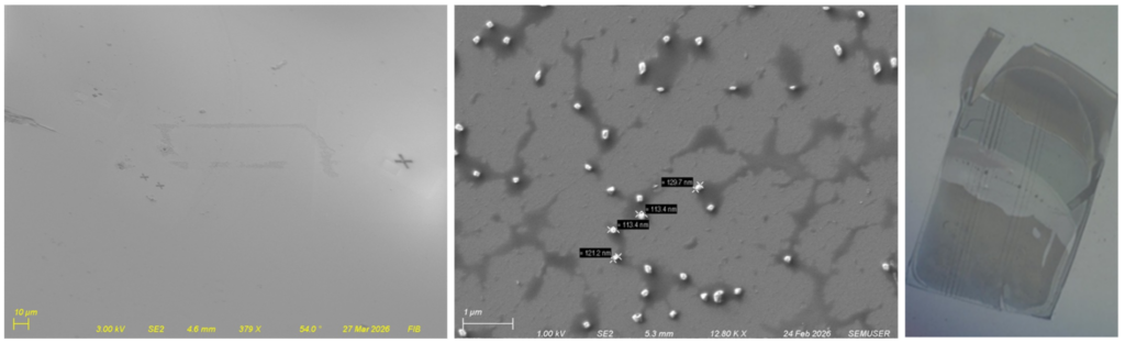
SIN after fs-laser treatment (Fig. 2, left): A 180 nm layer of SiN was deposited by a low-pressure CVD onto a 750 nm SiO2 layer prepared by a thermal wet oxidation on a Si-wafer. A PHAROS laser with ~100 fs pulse duration and 0.5 Hz pulse rep. rate was used for treatment of this sample during a few seconds. We used operation at 575-630 nm wavelengths, ~500 nJ energy per pulse, and ~3-μm beam diameter. Fig. 2, left shows a SEM micrograph with a treated area of a rectangle shape (~100 μm length).
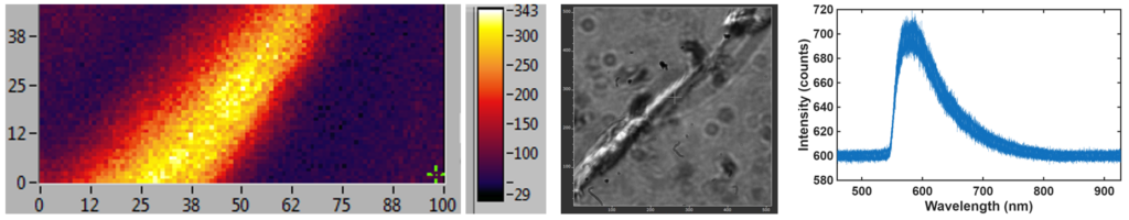
Silver nanocubes (Fig. 2, center): A sample with drop-casted silver nanocubes (NanoXast from nanoComposix) was used without any preliminary laser treatment. Fig. 2, center shows SEM micrograph of these 100 nm silver nanocubes coated by a few nm of polyvinylpyrrolidone (PVP) for protection from environment.
Silicone hydrogel after fs-laser treatment (Fig. 2, right): A silicone based contact lens hydrogel (Bausch & Lomb) was treated by a 515 nm, ~150 fs-laser to write lines at 50 μm below the surface (10 mm/s scan speed, 60 nJ per pulse 1,800 pulses, 3 μm diameter at laser power ~600 mW, 10 MHz pulse rep. rate).
EXPERIMENTAL SETUP: single-emitter confocal fluorescence microscopy and spectroscopy
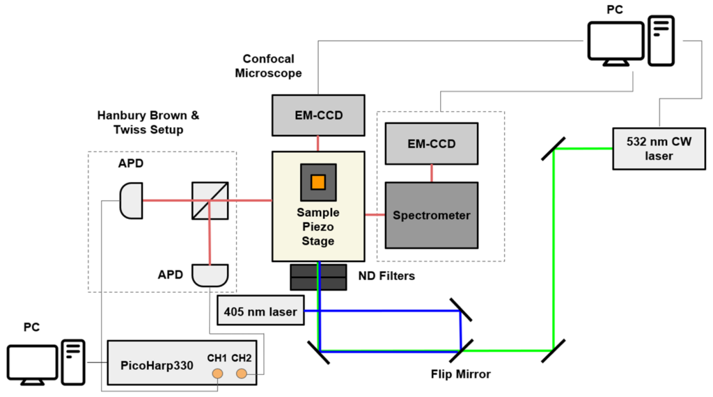
Fig. 3, shows a schematic of a confocal fluorescence microscope (oil-immersion objective with NA = 1.3) with a Hanbury Brown and Twiss interferometer and a low light spectrometer equipped with an EM-CCD. Two single-photon counting avalanche photodiode modules (APDs) were used as single-photon detectors. Two CW lasers with wavelengths of 405 nm and 532 nm were used for single-emitter excitation. PicoHarp330 single-photon counting electronics was used for antibunching measurements. For wide-field microscopy a second EM-CCD was used.
RESULTS 1: SiN with fs-laser written color centers


RESULTS 2: 100-nm silver nanocubes under 405 & 532 nm laser excitations
Usually, metal silver has a weak wide photoluminescence spectrum uniform along the sample surface, but in Ref. 3 appearance of photoluminescence centers with a single-emitter behavior was observed in a raster scan of the sample with 100 nm silver nanocubes widely used in plasmonic gap nanoantennas. Time traces of count rates from these centers showed bright intensity spikes and a step-wise count increase under higher 532 nm or 633 nm CW laser excitation. This section is devoted to further investigation of this effect under 405 nm or 532 nm CW laser excitation.
405 nm excitation:

532 nm excitation:

RESULTS 3: Silicone based contact lens gel polymer after fs-laser treatment
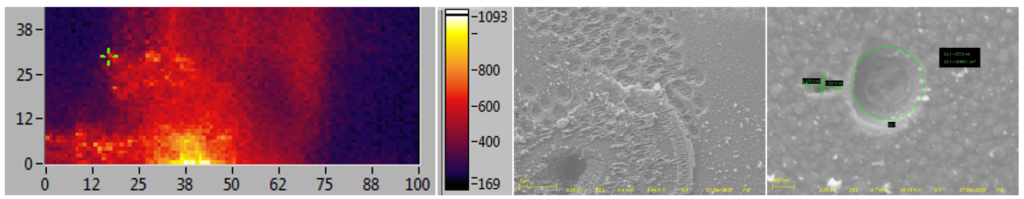
This part of the work was done to investigate polymers’ behavior after fs-laser treatment. Polymers are used in SPS applications as the spacers between nanoemitters and plasmonic nanostructures. For this part of our research we used a fs-treated polymer sample (silicone based contact lens hydrogel) as a part of research of W. Knox’s laboratory. Fig. 9 shows confocal fluorescence microscope raster scan image of a fs-treated area (left, with a bright line with higher count rate). The same area of the sample is shown with a wide-field microscopy (center) with a cross that indicate a position of excitation laser beam (532 nm). A right part of this figure shows the spectrum of a fs-treated area.
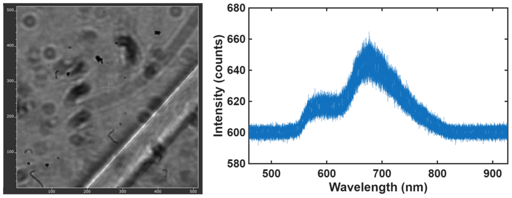
The main result of this research is that in the spectrum of a fs-laser treated area one of the maxima (680 nm) disappears after a fs-laser treatment. Fig. 10 shows a new position of a laser beam on the sample (indicated by a cross on the wide-field image on the left) that was moved to an untreated area. A right part of this figure shows a double maxima spectrum of an untreated area.
SUMMARY
The main results of this work:
(1) First demonstration of SPS based on a fs-induced color center in SiN.
(2) First demonstration of antibunching in plasmonic structures for SPS applications that can interfere with the main emitters placed into them for Purcell fluorescence enhancement.
(3) Observing spectral changes in photoluminescence of silicone based contact lens hydrogel after fs-laser treatment usually used for changing refractive index in it.
Acknowledgments
I would like to thank Prof. Svetlana Lukishova for supervising me for my senior thesis project as well as the Institute of Optics for support. I also want to thank Prof. Wayne Knox, Prof. Michele Cotrufo, Prof. Pablo Postigo, S. O’Neil, Q.R. Islam, M. Sanchez, X. Zhu, and M. Belzer for their help.
References
[1] S.G. Lukishova & L. J. Bissell. (2019). Nanophotonic Advances for Room-Temperature Single-Photon Sources. In: Boyd, R., Lukishova, S., Zadkov, V. (eds) Quantum Photonics,. Springer.
[2] XJ, Wang, HH. Fang, ZZ. Li, D. Wang, and H.B Sun, “Laser manufacturing of spatial resolution approaching quantum limit,” Light Sci Appl 13, 6 (2024).
[3] S.G. Lukishova, J. Brone, D. Khan, and Z. Li, “Ultrabright photoluminescence spikes and step-wise photoluminescence increase from colloidal silver nanoparticles for patch nanoantennas”, J. Phys.: Conf. Ser. Vol. 2249, 012002 (2022).