Team Roles
Primary Customer Contact: Johanna Cupp
Document Handler: Zachary Fox
Scribe: Sumedh Anantha
Customer

Advisor
Student/Faculty Advisor: Jacob Sacks
Customer Contacts
Marco Smarra and Athul Som
Introduction
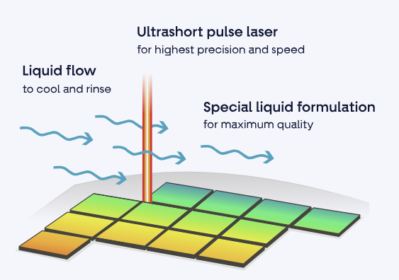
Semiconductor wafers must be diced with high precision. Defects such as chipping, cracking, and incomplete cuts are common in wafer dicing. Lidrotec’s system dices while the wafer is immersed in a specially formulated fluid. In-process imaging is needed to monitor cut quality during processing.
Lidrotec requested a compact multi-configuration camera system for semiconductor wafer inspection during dicing. The goal of this project was to design, build, and test a multi configuration imaging system capable of both wide and small field imaging, interfacing with Lidrotec’s current dicing system.
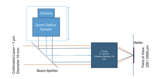
Lidrotec’s system requires imaging at two scales, a large field for alignment and monitoring, and a small field for resolving fine defects. This creates a challenging problem requiring high resolution imagery over both the wide and small field in one multiconfiguration system.The final prototype was designed for 650 nm operation, and the entrance pupil diameter (dictated by the f-ፀ lens) is 14 mm. The sensor choice, and therefore the magnifications and focal lengths, was left to our design team.
Design Exploration
Several design paths were considered at the beginning of the project. A reflective design was first explored due to its potential to reduce the package size. However, this approach would have required expensive custom aspheric mirrors and was impractical for the project timeline.
A commercial zoom camera plus relay design was also considered. This option would have made automated zooming easier by using a commercial zoom lens. However, the available zoom lenses were expensive and overdesigned for our application.
We then focused on refractive designs using both custom optics and stock lenses. Custom optical designs gave stronger performance, especially over the larger field of view, but the fabrication lead times were too long for project window. Because the project required a working proof of concept by the end of the semester, the stock optic path became the main build direction.
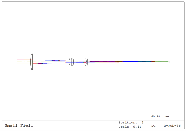
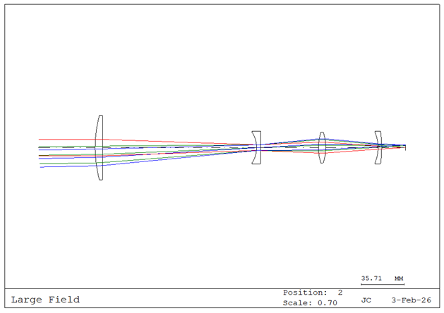
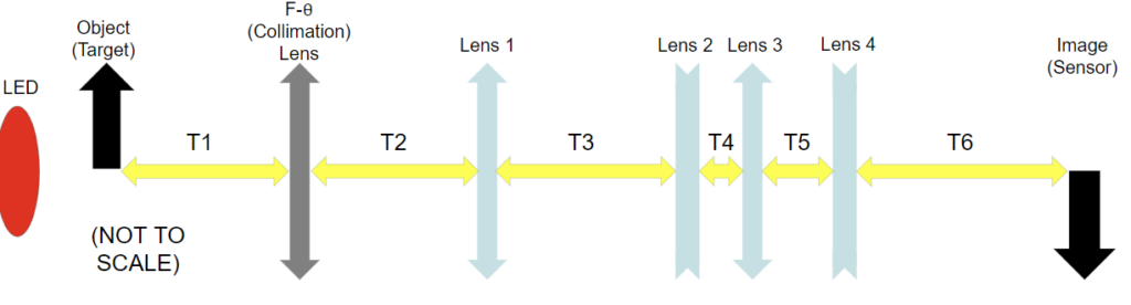
Prototype Design
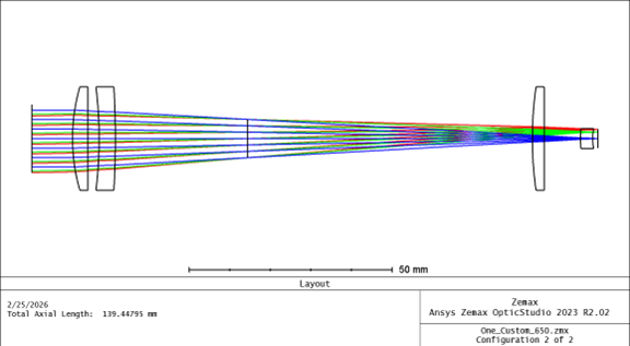
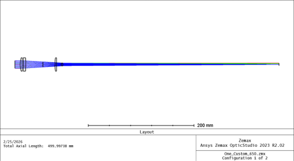
The prototype system was therefore based on the stock lens design, as it enabled the fastest timeline for developing a functional proof-of-concept. Diagrams of the stock system, along with performance metrics for both configurations, are shown below.
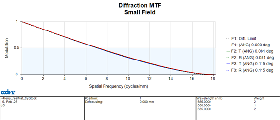

Performance Comparison and Trade-Offs
The custom design demonstrated significantly improved performance, particularly across the larger field of view. The small field region was diffraction-limited, while the large field approached diffraction-limited performance. Notably, comparable performance was achieved by replacing a single stock optic with a custom element, suggesting a potential lower-cost alternative to a fully custom system for Lidrotec. However, extended fabrication lead times rendered the fully custom design impractical within the project timeline.
Testing and Results
System Assembly
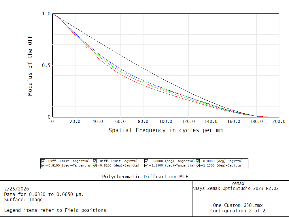
The prototype was aligned using a HeNe laser and iris targets. After alignment, the system was tested using a slant edge target, and the experimental MTF was analyzed in MATLAB. This allowed us to compare the nominal design to the as built prototype.

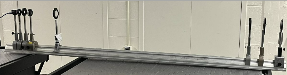
Figures 11-12 – Tested small field (top) and large field (bottom) configurations of the stock design
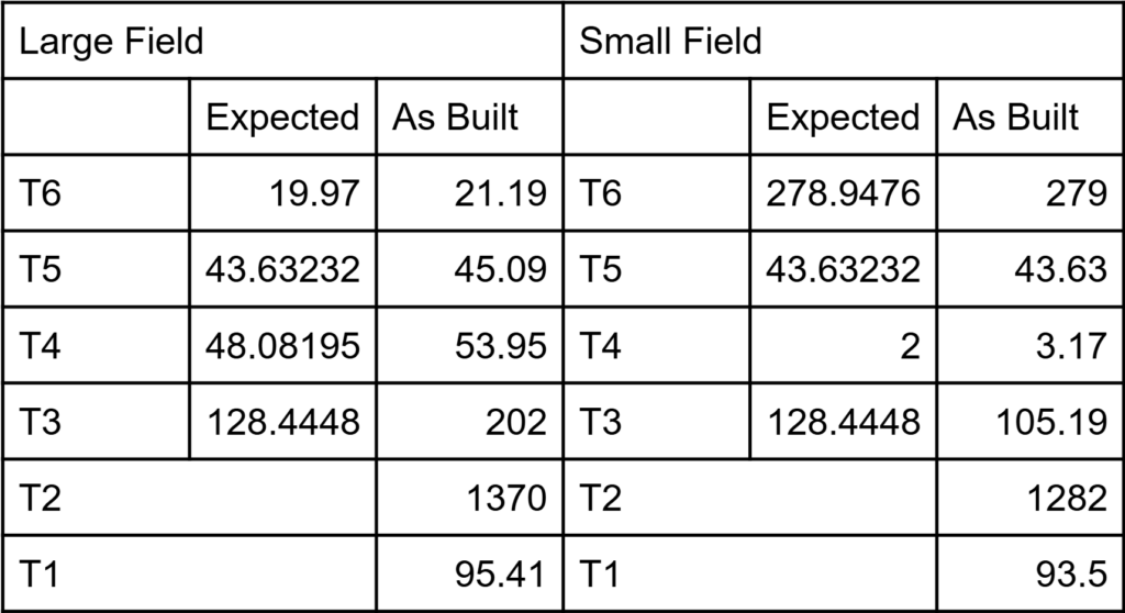
During alignment, some refocusing shifts were needed. The final lens positions did not perfectly match the expected design spacings, which is important when interpreting the measured performance. These adjustments were expected to affect the final MTF results, especially in the smaller field configuration where alignment is more sensitive. Such changes are outlined in the figure and table below.
Results
For as-built design analysis, both large and small fields MTF plots were averaged across fields. The large field MTF shows that the nominal design performs similarly to the as-built system, with >30% MTF at 16 lp/mm for the as-built compared to 13 lp/mm for the nominal design. This may be due to the system realignment outlined above or the field averaging, as the worst field’s performance was listed for the nominal design.
The small field nominal design is diffraction-limited, but the as-built system drops off more quickly, with >30% MTF at 5 lp/mm compared to 10 lp/mm for the nominal design, showing a clear drop off in performance. This is likely due to misalignment of the system.

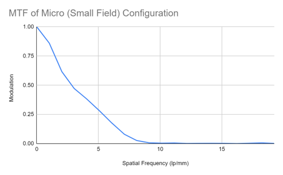
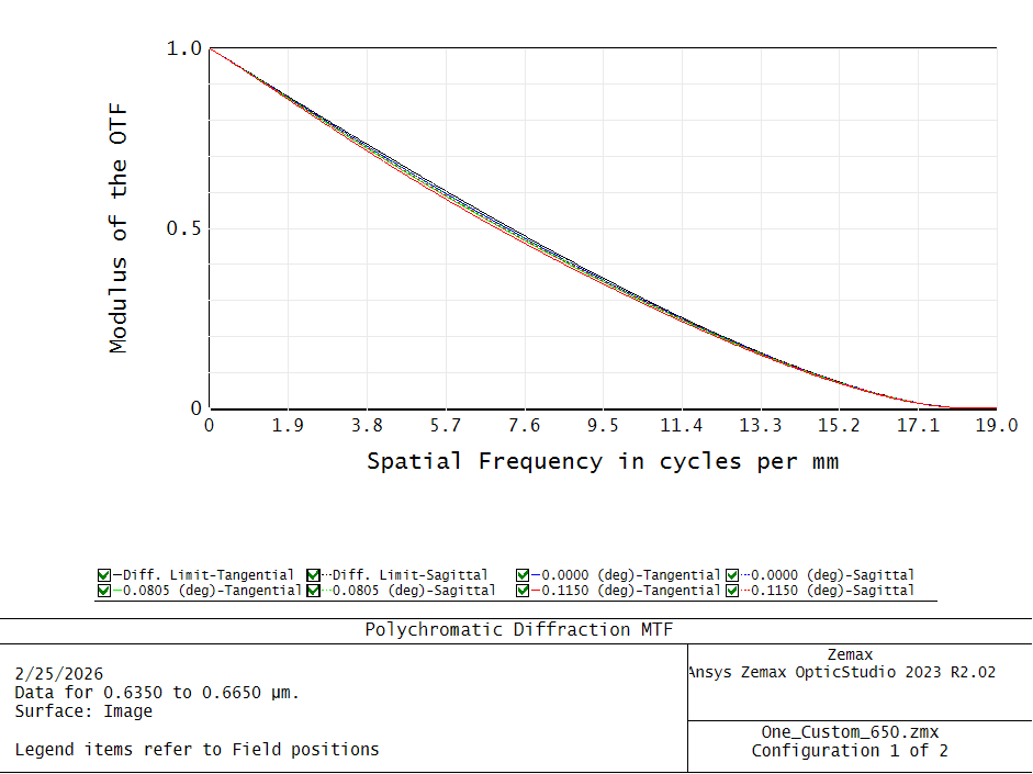
Figures 14-15: Nominal (left) and as-built (right) MTF performance for small field design
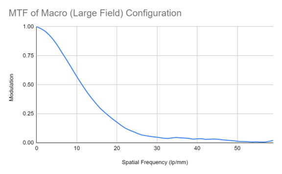
Figures 16-17: Nominal (left) and as-built (right) MTF performance for large field design
Conclusions
A multi-configuration zoom system was designed and prototyped for wafer inspection during dicing.
The final prototype was designed using stock optics and anyalzed using a slant edge target. It demonstrated a functional proof of concept for zoom functionality.
Despite reduced performance in certain fields the system provided a general foundation that can be improved upon with a better time frame
Future work could improve performance with custom optics, improved packaging, and implementing automated switching.
References
- LIDROTEC,” Lidrotec.com, 2023. https://lidrotec.com/.
- “U3-3131ACP Rev.1.2” IDS, https://en.ids-imaging.com/store/u3-33d0xcp-rev-1-2.html.